JAJU528B August 2022 – January 2023 OPA388-Q1
- 概要
- リソース
- 特長
- アプリケーション
- 5
- 1System Description
- 2System Overview
- 3Hardware, Testing Requirements, and Test Results
- 4Design Files
- 5Software Files
- 6Related Documentation
- 7Trademarks
- 8Revision History
2.2.2 AMC1301-Q1
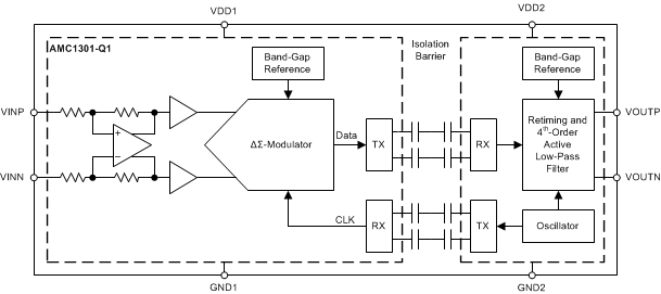
The AMC1301 device is a fully-differential, precision, isolated amplifier. The input stage of the device consists of a fully-differential amplifier that drives a second-order, delta-sigma (ΔΣ) modulator. The modulator uses the internal voltage reference and clock generator to convert the analog input signal to a digital bit stream. The drivers transfer (TX) the output of the modulator across the isolation barrier that separates the high-side and low-side voltage domains. The received bit stream and clock are synchronized and processed by a fourth-order analog filter on the low-side and presented as a differential output of the device.
Figure 2-4 shows the AMC1301-Q1 block diagram.
 Figure 2-4 AMC1301-Q1 Block
Diagram
Figure 2-4 AMC1301-Q1 Block
DiagramThe SiO2-based, double-capacitive isolation barrier supports a high level of magnetic field immunity, as described in ISO72x Digital Isolator Magnetic-Field Immunity . The digital modulation used in the AMC1301 device and the isolation barrier characteristics result in high reliability and common-mode transient immunity (CMTI).
Key features include:
- ±250-mV input voltage range optimized for current measurement using shunt resistors
- Fixed gain: 8.2
- Very low gain error and drift: ±0.3% at 25°C, ±50 ppm/°C
- Very low nonlinearity and drift: 0.03%, 1 ppm/°C
- System-level diagnostic features