JAJU648A November 2018 – April 2022 TLV3601 , TLV3601-Q1 , TLV3603 , TLV3603-Q1
- 概要
- Resources
- 特長
- アプリケーション
- 5
- 1System Description
- 2System Overview
- 3Hardware, Software, Testing Requirements, and Test Results
- 4Design Files
- 5Related Documentation
- 6About the Author
- 7Revision History
2.2.3.1 Laser Driver and Laser Diode
The laser driver used in the design is an iC-HB, 155-MHz, triple-laser switch from iC-Haus™. See the Triple 155MHz Laser Switch data sheet for the recommended laser driver for this design. The recommended laser diode is a 1550-nm distributed feedback laser (DFB) LDM5S515-015 from OEQuest™. In a pulsed high-speed application, toggling a laser on and off causes suboptimal performance. Rather than turning the laser off, configure the laser to just less than its turnon threshold when the laser is inactive to ensure a smoother and quicker turnon. This configuration minimizes the effects of parasitic capacitances that require charging and discharging during transient operation.
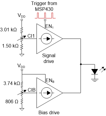
Figure 2-2 shows a simplified schematic of the laser setup. See Figure 4-2 for the complete printed circuit board (PCB) schematic. Consider each channel of the laser-diode driver to be a voltage-controlled current source (VCCS) with an enable and disable switch. The three parallel channels are as follows:
- The bias channel sets the laser at its threshold condition
- Channel 1 drives the signal current that toggles the laser on or off
- Channel 2 is unused in this application
 Figure 2-2 Laser Diode Block Diagram
Using the onboard resistor divider and potentiometer subcircuit connected between the 5-V supply and ground sets the bias voltage to control the VCCS. Set the bias supply to 1.15 V and the signal supply on channel 1 to 1.65 V. The jumper statically controls the bias channel state and the trigger generated by the MPS430 controls the signal channel. The adjustable linear regulator (U3) is configured to drive an output voltage of 3.3 V on the 3p3V line. This voltage drives the primary side of the SN74LVC1T45 logic-level translator to shift the 0-V to 3.3-V logic level from the trigger signal of the MSP430 to a 0-V to 5-V digital signal required to drive the iC-HB device. For more information, see Figure 2-1.