SBOA571 august 2023 OPA2387 , OPA387 , OPA4387
3.2 Second Order Shelving Filter
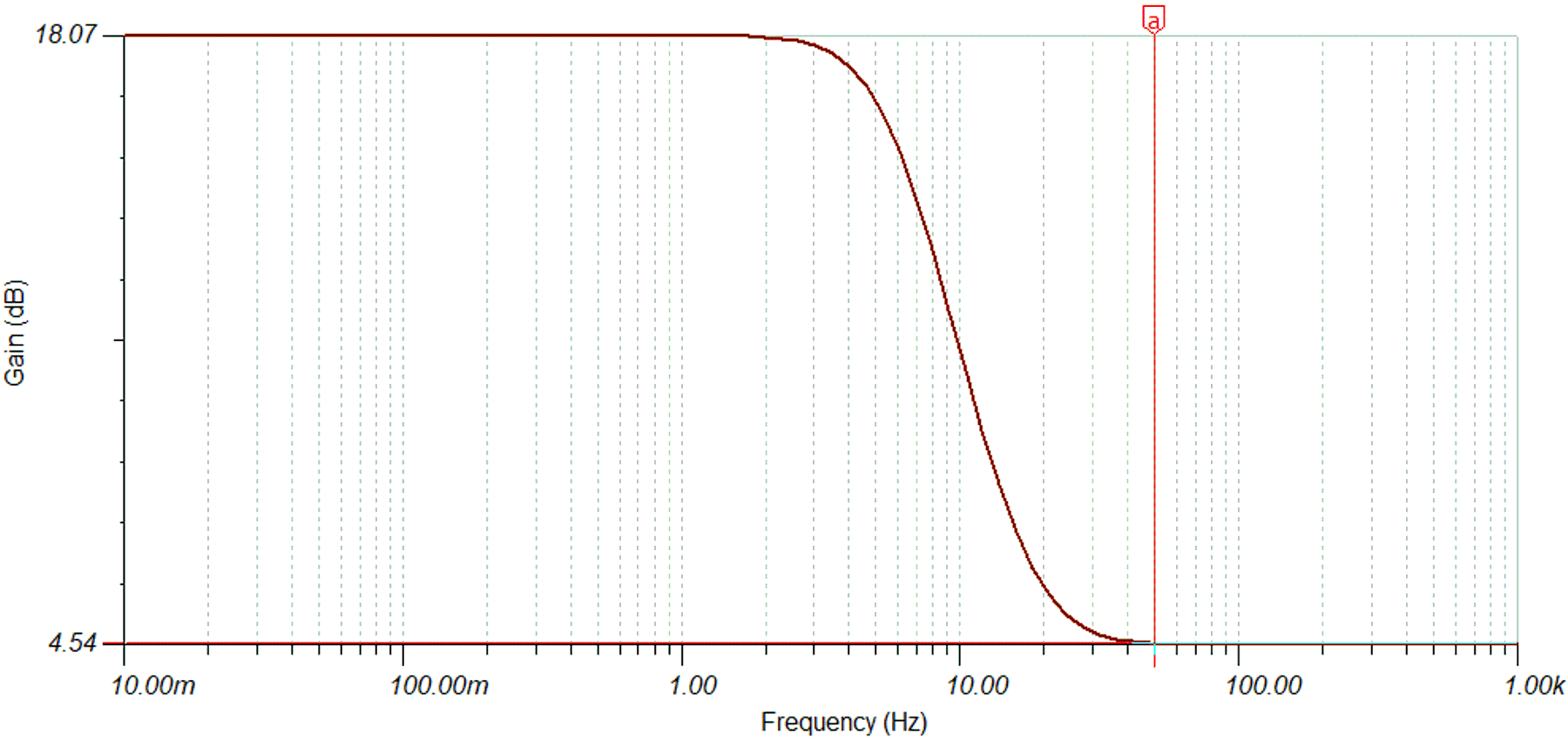
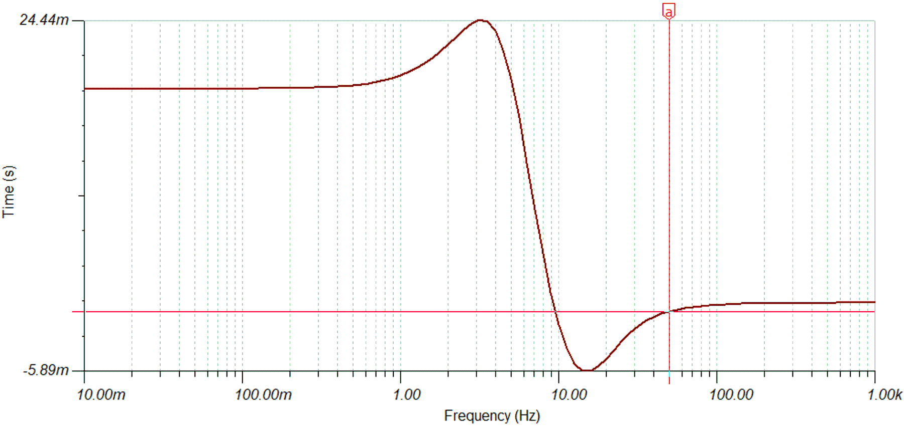
Improvements can be achieved by introducing the suggested second order shelving filter. Due to the additional pole, a much faster group delay at DC can be achieved in the range of 20 ms. The frequency plot indicates a smaller transition band between DC and AC allowing to position this at a higher frequency closer to the AC passband and to detect the change in DC (wander) much faster. Again, the circuit incorporates a matching resistor divider at the non-inverting input to reduce the Ib current based offset error. The shown filter structure is an inverting structure. The output polarity is reversed.
 Figure 3-6 Second Order Shelving Filter Circuit
 Figure 3-7 Frequency Response of the Second Order Shelving Filter
 Figure 3-8 Group Delay of the Second Order Shelving Filter
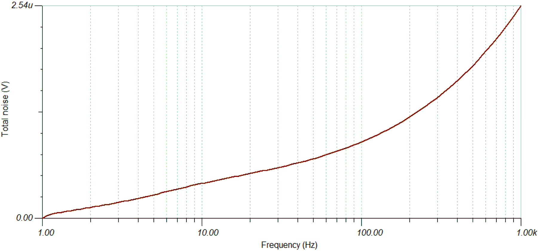
 Figure 3-9 Total Output Noise of the Second Order Shelving Filter