SLOA292 May 2020 TAS5760LD
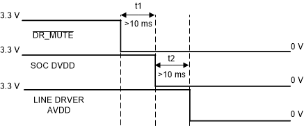
3.1 Power Down Sequence
- Mute TAS5760 HP.
- Turn down SOC 3.3 V (output impedance keeps low. It can avoid pop).
- Shutdown HP 3.3 V.
 Figure 3. Line Driver Power Sequence
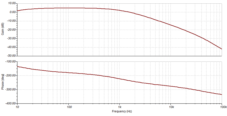
 Figure 4 is frequency response TINA simulation of the typical line drive circuit (subwoofer stereo to mono line driver). The frequency response from 20Hz to approximately 200Hz is within ±3dB range.
 Figure 4. Frequency Response of Typical Subwoofer Line Driver Stereo to Mono Circuit
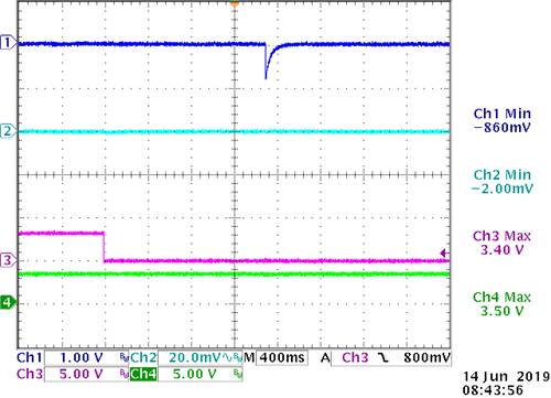
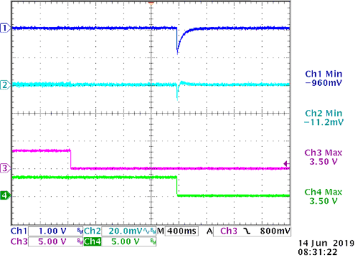
 In Figure 5, the big DC level transient at the line driver input, but there is no transient voltage at line driver output. The reason is SOC 3.3 V power and line driver 3.3 V power are separated. The line driver 3.3 V power was not provided while there is big DC level transient from SOC's output. Figure 6 shows that the case SOC and line driver share the same 3.3 V power supply. The voltage drop in channel 1 due to 3.3 V power supply for SOC and line driver turns off at the same time. Channel 2‘s waveform shows the line driver of TAS5760LD output transient around -11mV. CH1 is input from SOC. R CH2 is line driver output. CH3 is (DR_MUTE )̅ controlled waveform by SOC’s GPIO. CH4 is 3.3V for line driver power.
 Figure 5. TAS5760LD Line Driver's Waveform With Proper Power Sequence
  Figure 6. TAS5760LD Line Driver's Waveform With Improper Power Sequence