SLVUBO3A April   2019  – October 2020 TPS650330-Q1


  1.   Trademarks
  2. 1BOOSTXL-TPS65033 Components and Environment
  3. 2BOOSTXL-TPS65033 Board Information
    1. 2.1 Critical Socketed Board Connections
      1. 2.1.1 Power Switches
    2. 2.2 Jumpers and Test Points
  4. 3Programming GUI Operation
    1. 3.1 Initial Set-up
      1. 3.1.1 Finding the GUI
      2. 3.1.2 Offline Installation
      3. 3.1.3 Flashing the MSP430F5529 LaunchPad
      4. 3.1.4 Flashing the MSP432E401Y Launch Pad
    2. 3.2 Connection Debugging
    3. 3.3 Basic Operation of the GUI
      1. 3.3.1 Home
      2. 3.3.2 Block Diagram
      3. 3.3.3 Registers
      4. 3.3.4 Device Configuration
        1. 3.3.4.1 Using Device Configuration to Define Spin Settings
        2. 3.3.4.2 Configuring the Power Sequence
    4. 3.4 Scripting
  5. 4Recommended Operating Procedure
  6. 5BOOSTXL-TPS65033 Schematic
  7. 6BOOSTXL-TPS65033 Board Layers
  8. 7BOOSTXL-TPS65033 Bill of Materials
  9. 8Revision History

Configuring the Power Sequence

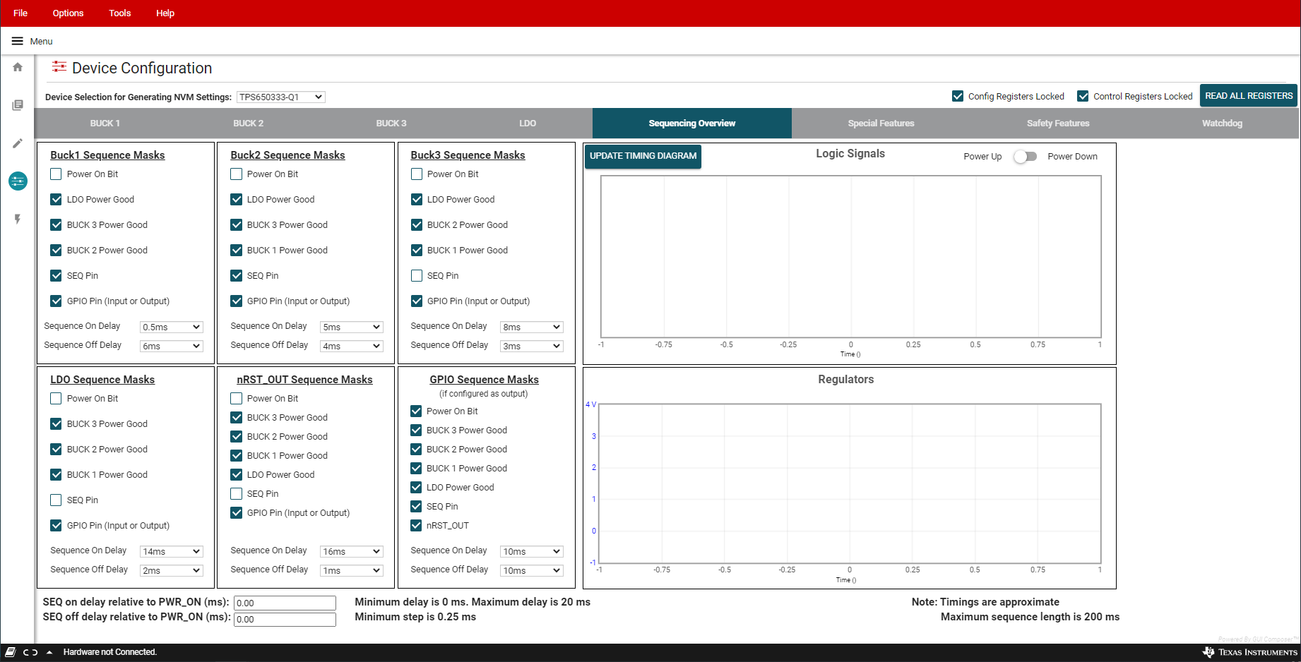
The Sequencing Overview tab includes instruments to customize the power sequence of the PMIC. Note that the check boxes are power sequence masks. If a particular logic signal needs to be included as part of the regulator or logic power up sequence, leave the box next to the logic signal unchecked. TI recommends to set Power On Bit unmasked for each rail that is required in the application.
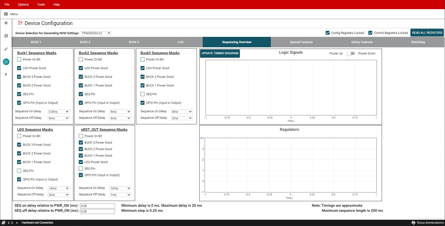
GUID-20200915-CA0I-BRTR-QZLP-1D84XVD20V5L-low.pngFigure 3-18 Sequencing Overview Tab
When using a TPS65033x-Q1 device, the GPIO pin can also be used for power sequencing of an external regulator or other device. In the Special Features tab, configure GPIO as an output to include its sequencing in the Sequencing Overview tab. Note that when using GPIO for sequencing, the GPIO Function must be Enabled.
GUID-20200915-CA0I-PSX6-3V8D-TZFSSHV1DTNN-low.pngFigure 3-19 Sequencing Overview Including GPIO
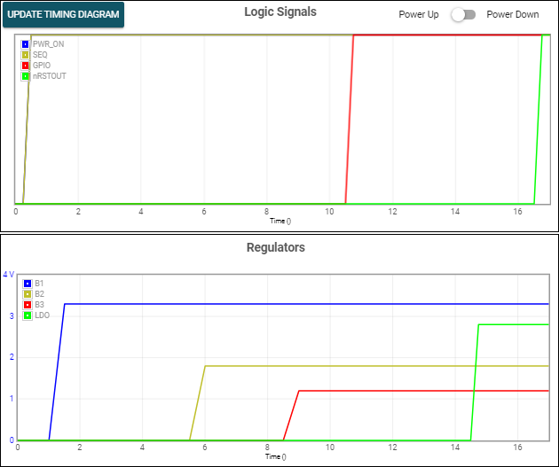
For reference, the GUI can generate example power-up and power-down timing diagrams based on the sequence settings present when the UPDATE TIMING DIAGRAM button is clicked. As noted, rise and fall times are approximate, and the maximum sequence length is 200 ms. Changes to regulator enable and output discharge settings are reflected in the timing diagram. If the sequence settings are not valid, the GUI will provide a notifying message and the timing diagram will not be updated. For example, if a regulator is enabled but fails to power-up within 200 ms, the sequence settings are not valid.
GUID-20200915-CA0I-GXKH-Q8ZJ-L9ZDQ98TKD45-low.pngFigure 3-20 GUI Generated Timing Diagram