SLVUBO3A April   2019  – October 2020 TPS650330-Q1


  1.   Trademarks
  2. 1BOOSTXL-TPS65033 Components and Environment
  3. 2BOOSTXL-TPS65033 Board Information
    1. 2.1 Critical Socketed Board Connections
      1. 2.1.1 Power Switches
    2. 2.2 Jumpers and Test Points
  4. 3Programming GUI Operation
    1. 3.1 Initial Set-up
      1. 3.1.1 Finding the GUI
      2. 3.1.2 Offline Installation
      3. 3.1.3 Flashing the MSP430F5529 LaunchPad
      4. 3.1.4 Flashing the MSP432E401Y Launch Pad
    2. 3.2 Connection Debugging
    3. 3.3 Basic Operation of the GUI
      1. 3.3.1 Home
      2. 3.3.2 Block Diagram
      3. 3.3.3 Registers
      4. 3.3.4 Device Configuration
        1. 3.3.4.1 Using Device Configuration to Define Spin Settings
        2. 3.3.4.2 Configuring the Power Sequence
    4. 3.4 Scripting
  5. 4Recommended Operating Procedure
  6. 5BOOSTXL-TPS65033 Schematic
  7. 6BOOSTXL-TPS65033 Board Layers
  8. 7BOOSTXL-TPS65033 Bill of Materials
  9. 8Revision History

Block Diagram

The Block Diagram section displays the typical components and functional blocks of the PMIC. A block diagram for the Programming BoosterPack is also shown.
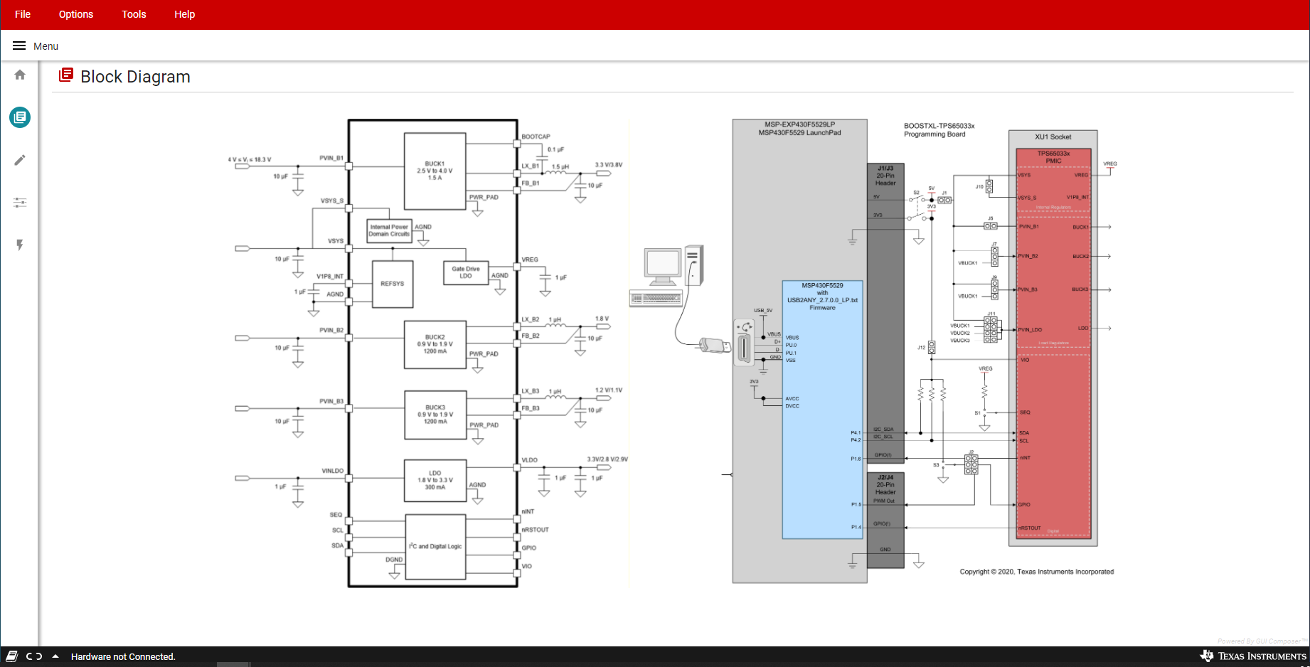
GUID-20200921-CA0I-9W1K-PX30-MFQ8NQ8RFFW5-low.pngFigure 3-13 TPS6503xx-Q1 GUI Block Diagram Page