SLVUBQ1A August 2020 – May 2021 TPS543620
- Trademarks
- 1Introduction
- 2Configurations and Modifications
-
3Test Setup and Results
- 3.1 Input/Output Connections
- 3.2 Efficiency
- 3.3 Output Voltage Regulation
- 3.4 Load Transient and Loop Response
- 3.5 Output Voltage Ripple
- 3.6 Input Voltage Ripple
- 3.7 Synchronizing to a Clock
- 3.8 Start-up and Shutdown with EN
- 3.9 Start-up and Shutdown with VIN
- 3.10 Start-up Into Pre-Bias
- 3.11 Hiccup Current Limit
- 3.12 Overvoltage Protection
- 3.13 Thermal Performance
- 4Board Layout
- 5Schematic and Bill of Materials
- 6Revision History
3.2 Efficiency
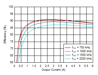
Figure 3-1 through Figure 3-5 show the efficiency for both designs on the TPS543620EVM. Using the selection jumpers for U2, the results for different output voltage and switching frequency combinations are included. The test points listed in Table 3-3 are used for the efficiency measurement. Use these test points to minimize the contribution of PCB parasitic power loss to the measured power loss.
The following are some additional test setup considerations to minimize external sources of power dissipation.
- Disable the other regulator to avoid including the switching quiescent current of the other regulator in the efficiency measurement. When testing U1 with U2 disabled, an external power supply should be used to power the buffer connected to the FSEL pin as described in this note.
- Do not measure the SW pin of U2 with TP28 while measuring the efficiency of U2. Measuring the SW pin with this test point loads this node with 500 Ω and the efficiency measurement will include the power lost in this external resistance.
- Remove the shunts from J11 and J13 as a small amount of power is dissipated in the EN resistor divider connected to U2.
Table 3-3 Efficiency Measurement Test
Points
| RELATED IC | TEST POINT NAME | REFERENCE DESIGNATOR | FUNCTION |
|---|---|---|---|
| U1 | VIN_U1 | TP1 | Input voltage test point connected near pins of U1 |
| VOUT_U1 | TP2 | Output voltage test point near output inductor of U1 | |
| PGND_EFF_U1 | TP5 | PGND reference test point for both input and output voltages Kelvin connected near U1 | |
| U2 | VIN_U2 | TP12 | Input voltage test point connected near pins of U2 |
| VOUT_U2 | TP15 | Output voltage test point near output inductor of U2 | |
| PGND_EFF_U2 | TP17 | PGND reference test point for both input and output voltages Kelvin connected near U2 |
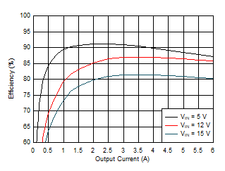
| VOUT = 1 V | fSW = 1500 kHz |
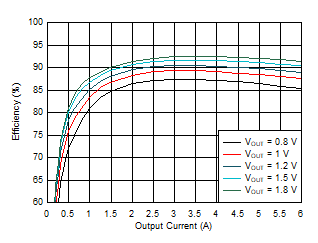
| VIN = 12 V | fSW = 1000 kHz |
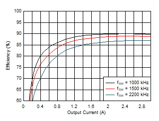
| VIN = 9 V | VOUT = 1 V | RMODE = 60.4 kΩ |
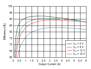
| VOUT = 1 V | fSW = 1000 kHz |

| VIN = 9 V | VOUT = 1 V |