SLVUBQ1A August 2020 – May 2021 TPS543620
- Trademarks
- 1Introduction
- 2Configurations and Modifications
-
3Test Setup and Results
- 3.1 Input/Output Connections
- 3.2 Efficiency
- 3.3 Output Voltage Regulation
- 3.4 Load Transient and Loop Response
- 3.5 Output Voltage Ripple
- 3.6 Input Voltage Ripple
- 3.7 Synchronizing to a Clock
- 3.8 Start-up and Shutdown with EN
- 3.9 Start-up and Shutdown with VIN
- 3.10 Start-up Into Pre-Bias
- 3.11 Hiccup Current Limit
- 3.12 Overvoltage Protection
- 3.13 Thermal Performance
- 4Board Layout
- 5Schematic and Bill of Materials
- 6Revision History
2.1 Output Voltage
In the U1 design, the output voltage is set by the resistor divider network of R7 (RFBT) and R8 (RFBB). R8 is fixed at 1.00 kΩ to set the FB divider current at approximately 500 µA. To change the output voltage of the EVM, the value of resistor R7 must change. Changing the value of R7 can change the output voltage above the 0.5-V reference voltage (VREF). The value of R7 for a specific output voltage can be calculated using Equation 1. After changing R7, the feedfoward capacitor (C8) can also need to be changed.
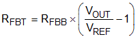
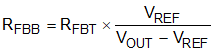
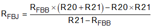
In the U2 design, there are a few ways to set the output voltage. First, jumper J14 can be used to select between the options shown in Table 2-1. If the desired output voltage is not available, a resistor must be changed. For output voltages less than 0.8 V, TI recommends leaving J14 open and increasing R21. R21 becomes RFBB and the required value for can be calculated with Equation 2, where RFBT is R15. For output voltages greater than 0.8 V, the jumper output voltage options can be changed by changing one of the resistors R23-R26. The RFBJ resistor value to get a desired equivalent RFBB resistance can be calculated with Equation 3. To use J14 for output voltages 3.3 V or larger, R20 should be reduced to 499 Ω.
| JUMPER SETTING | EQUIVALENT BOTTOM FB RESISTOR (RFBB) | NOMINAL OUTPUT VOLTAGE |
|---|---|---|
| Open | R21 = 8.25 kΩ | 0.803 V |
| 1 to 2 pin shorted(1) | (R23+R20)||R21 = 4.97 kΩ | 1.003 V |
| 3 to 4 pin shorted | (R24+R20)||R21 = 3.55 kΩ | 1.204 V |
| 5 to 6 pin shorted | (R25+R20)||R21 = 2.48 kΩ | 1.507 V |
| 7 to 8 pin shorted | (R26+R20)||R21 = 1.92 kΩ | 1.803 V |