SNLA113C november 2008 – june 2023 DS91M124 , DS91M125 , SN65LVDM050 , SN65LVDM050-Q1 , SN65LVDM051 , SN65LVDM051-Q1 , SN65LVDM1676 , SN65LVDM1677 , SN65LVDM176 , SN65LVDM179 , SN65LVDM180 , SN65LVDM22 , SN65LVDM31 , SN65MLVD040 , SN65MLVD047A , SN65MLVD048 , SN65MLVD080 , SN65MLVD082 , SN65MLVD128 , SN65MLVD129 , SN65MLVD2 , SN65MLVD200A , SN65MLVD202A , SN65MLVD204A , SN65MLVD204B , SN65MLVD206B , SN65MLVD3
- 1
- AN-1926 An Introduction to M-LVDS and Clock and Data Distribution Applications
- Trademarks
- 1 Introduction
- 2 M-LVDS Standard Overview
- 3 Driver Characteristics
- 4 Receiver Characteristics
- 5 M-LVDS Portfolio
- 6 M-LVDS Applications
- 7 Clock Distribution in AdvancedTCA Systems
- 8 Clock Distribution in MicroTCA Systems
- 9 M-LVDS as a Short Reach RS-485 Alternative
- 10Signal Distribution with Point-to-Point Links
- 11Wired-OR Implementation
- 12Design Guidelines
- 13Conclusion
- 14References
- 15Revision History
4 Receiver Characteristics
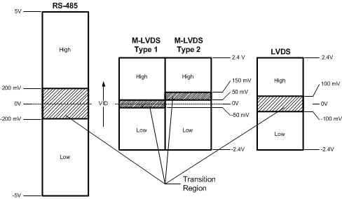
The key receiver specifications are input voltage threshold, input common mode range, and input leakage current. The input threshold levels differentiate the two types of M-LVDS receivers. Type 1 receivers have threshold levels centered at 0V differential and provide higher noise margin than Type 2 receivers. Type 1 receivers are used in clock or data transmission applications that either require application specific external failsafe networks or don’t require failsafe provisions at all. Type 2 receivers have threshold levels shifted by +100 mV differential. The shift lowers noise margin but provides a known, low output state when a bus or a transmission line is undriven and having 0V differential bias. In addition to the failsafe, Wired-OR function is another possible application of Type 2 receivers. More information about the Wired-OR implementation using M-LVDS devices is given later in the note.
When compared to RS-485 and LVDS receivers, M-LVDS receivers have the tightest threshold levels. Figure 4-1 illustrates threshold levels and maximum recommended differential input amplitude levels of RS-485, LVDS, and both M-LVDS receivers.
 Figure 4-1 M-LVDS Standard Defines Two
Receiver Types
Figure 4-1 M-LVDS Standard Defines Two
Receiver TypesThe M-LVDS receiver input common mode range of –1.4V to 3.8V makes M-LVDS a robust interface for connecting sub-systems that may have a potential difference between their ground references of ±1V. Given the fact that many M-LVDS drivers have a much tighter VOS specification than what the standard specifies, the unwanted potential difference between network nodes may be greater than ±1V. RS-485 receivers are suitable for even harsher environments. Their common mode range of −7V to 12V allows for ±7V of unwanted potential difference between the nodes. The LVDS receivers pose as the least robust receivers given their input common mode range of 0V to 2.4V (0 to VDD is also very common), however, tight VOS specification of LVDS drivers allows a potential difference between driver and receiver circuit commons of ±1V.
As all M-LVDS, LVDS and RS-485 devices may be used in multipoint networks, the receivers have to pose as light loads to the active drivers so that many of them can be connected on a single bus. Based on this requirement, all three standards specify maximum input leakage current which allows up to 32 loads (receivers or inactive drivers) on a bus. A load of a single device or one unit load for M-LVDS and LVDS receivers is equivalent to a 120 kΩ resistor into a 0V to 2.4V voltage source. One unit load for an RS-485 receiver is equivalent to a 12 kΩ resistor into a 0V to 5V source. In addition, the RS-485 devices are available in 1/2, 1/4 and 1/8 unit loads allowing up to 256 devices on a bus. Table 4-1 shows key RS-485, M-LVDS and LVDS receiver characteristics.
| Parameter | RS-485 | M-LVDS | LVDS |
|---|---|---|---|
| VID (V) | 0.4 to 5.0 | 0.1 to 2.4 | 0.2 to 2.4 |
| VCM (V) | −5.0 to 12.0 | −1.4 to 3.8 | 0 to 2.4 |
| IIN (µA) | <1000 | <32 | <20 |