SNLA113C november 2008 – june 2023 DS91M124 , DS91M125 , SN65LVDM050 , SN65LVDM050-Q1 , SN65LVDM051 , SN65LVDM051-Q1 , SN65LVDM1676 , SN65LVDM1677 , SN65LVDM176 , SN65LVDM179 , SN65LVDM180 , SN65LVDM22 , SN65LVDM31 , SN65MLVD040 , SN65MLVD047A , SN65MLVD048 , SN65MLVD080 , SN65MLVD082 , SN65MLVD128 , SN65MLVD129 , SN65MLVD2 , SN65MLVD200A , SN65MLVD202A , SN65MLVD204A , SN65MLVD204B , SN65MLVD206B , SN65MLVD3
- 1
- AN-1926 An Introduction to M-LVDS and Clock and Data Distribution Applications
- Trademarks
- 1 Introduction
- 2 M-LVDS Standard Overview
- 3 Driver Characteristics
- 4 Receiver Characteristics
- 5 M-LVDS Portfolio
- 6 M-LVDS Applications
- 7 Clock Distribution in AdvancedTCA Systems
- 8 Clock Distribution in MicroTCA Systems
- 9 M-LVDS as a Short Reach RS-485 Alternative
- 10Signal Distribution with Point-to-Point Links
- 11Wired-OR Implementation
- 12Design Guidelines
- 13Conclusion
- 14References
- 15Revision History
5 M-LVDS Portfolio
TI’s current M-LVDS product family consists of a wide array of devices ranging from single channel transceivers and driver/receiver pairs to quad channel transceivers, drivers and 1:4 repeaters/fan-out buffers.
The first generation of TI’s M-LVDS devices introduced in 2006 includes four single channel devices providing 100 MHz / 200 Mbps transceivers and driver/receiver pairs with Type 1 and Type 2 receiver options. Table 5-1 summarizes the available options. Detailed information on each device can be found at www.ti.com.
| Part Number | Description | Package | Features |
|---|---|---|---|
| DS91D176 | 100 MHz Single Channel M-LVDS Transceiver | SOIC-8 | `176 Pinout, Type 1 Receiver |
| DS91C176 | 100 MHz Single Channel M-LVDS Transceiver | SOIC-8 | `176 Pinout, Type 2 Receiver |
| DS91D180 | 100 MHz Single Channel M-LVDS Line Driver / Receiver Pair | SOIC-8 | `180 Pinout, Type 1 Receiver |
| DS91C180 | 100 MHz Single Channel M-LVDS Line Driver / Receiver Pair | SOIC-8 | `180 Pinout, Type 2 Receiver |
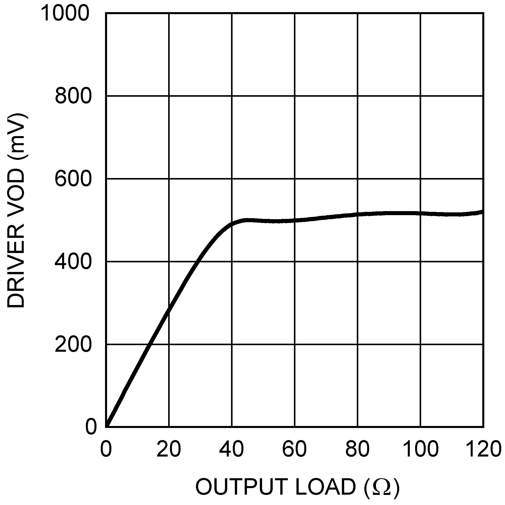
The first generation of M-LVDS devices features drivers with transition times (1.8 ns typ) optimized for multipoint networks, more specifically for ATCA clock distribution networks. In addition, the drivers feature output amplitude control circuitry that maintains constant VOD over a wide range of loads as illustrated in Figure 5-1. This feature helps with the noise margin in heavily loaded backplanes.
 Figure 5-1 DS91D176 Driver Output Amplitude as a Function of Output DC Load
The second generation of M-LVDS devices introduced in 2008 includes four quad channel 125 MHz / 250 Mbps devices. Table 5-2 summarizes the available options. Similar to the first generation, these devices also feature controlled transition times (2.0 ns typ) and output amplitude control circuitry for maintaining constant VOD over a wide range of loads.
| Part Number | Description | Package | Features |
|---|---|---|---|
| DS91M040 | 125 MHz Quad M-LVDS Transceiver | LLP-32 | Space saving package, pin settable receiver type, per channel output enable |
| DS91M047 | 125 MHz Quad M-LVDS Line Driver | SOIC-16 | `047 pinout, per channel output enable |
| DS91M124 | 125 MHz 1:4 M-LVDS Repeater with LVCMOS Input | SOIC-16 | Low skew, per channel output enable |
| DS91M125 | 125 MHz 1:4 M-LVDS Repeater with LVDS Input | SOIC-16 | LVDS input, per channel output enable |