SPRADF4 December 2023 TMS320F280023C , TMS320F280025C , TMS320F280025C-Q1 , TMS320F280037C , TMS320F280037C-Q1 , TMS320F280039C , TMS320F280039C-Q1 , TMS320F280049C , TMS320F280049C-Q1 , TMS320F28377D , TMS320F28377D-EP , TMS320F28377D-Q1 , TMS320F28377S , TMS320F28377S-Q1 , TMS320F28379D , TMS320F28379D-Q1 , TMS320F28379S , TMS320F28P650DK
4 Turn-Off Delay Configurations
The switching frequency is larger than the resonant frequency during resonant mode, and the current on the SR MOSFETs still exist after the primary side PWM turns off, as shown in Figure 1-1. Extending the on time for the SR PWM by adding the turn-off delay (normally within 200 ns) helps improve system efficiency. To add the turn-off delay, this report provides two configurations.
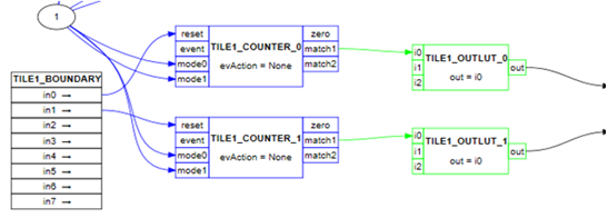
The first configuration option is to leverage an extra Counter 2 from another CLB tile (like CLB3).
The first step in this configuration is to set the CLB input IN0 and IN1 to use the falling edges of EPWM1A and EPWM1B to reset the related counter to 0 (Figure 4-1) and set the match 1 values to represent the required turn-off delay for SR PWM. The next step is to select the match 1 event of the Counter 2 as the output, which replaces the original CLB2 IN0 (falling edge of EPWM1A) and IN2 (falling edge of EPWM1B), respectively.
 Figure 4-1 First CLB Configuration
Option with Additional 2 Counters
Figure 4-1 First CLB Configuration
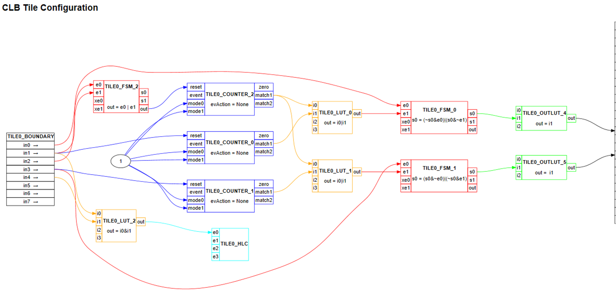
Option with Additional 2 CountersFor three-phase, interleaved LLC, there are not enough CLB tiles to provide the extra counters for the turn-off-delay design (Figure 4-1); however, using a second option that utilizes a single counter within the same CLB tile for the specific SR PWM is possible. In this second option (Figure 4-2), the falling edges of EPWM1A and EPWM1B (OR logic with LUT) are selected to reset the Counter 2 while the match 1 value is set with the expected delay timing. The important change for the CLB block diagram is replacing the IN0 inputs of LUT0 and LUT1 with the match 1 event of counter 2. With this option, the remaining FSM 2 works as the LUT function since all three LUT functions are occupied.
 Figure 4-2 Second CLB Configuration
Option with Single Counter