SPRUIW7A October 2020 – February 2022
- Trademarks
- 1Introduction
- 2J7200 EVM Overview
- 3EVM User Setup/Configuration
-
4J7200 EVM Hardware Architecture
- 4.1 J7200 EVM Hardware Top Level Diagram
- 4.2 J7200 EVM Interface Mapping
- 4.3 I2C Address Mapping
- 4.4 GPIO Mapping
- 4.5 Power Supply
- 4.6 Reset
- 4.7 Clock
- 4.8 Memory Interfaces
- 4.9 MCU Ethernet Interface
- 4.10 QSGMII Ethernet Interface
- 4.11 PCIe Interface
- 4.12 USB Interface
- 4.13 Audio Interface
- 4.14 CAN Interface
- 4.15 FPD Interface (Audio Deserializer)
- 4.16 I3C Interface
- 4.17 ADC Interface
- 4.18 RTC Interface
- 4.19 Apple Authentication Header
- 4.20 JTAG Emulation
- 4.21 EVM Expansion Connectors
- 4.22 ENET Expansion Connector
- 5Functional Safety
- 6Revision History
4.20 JTAG Emulation
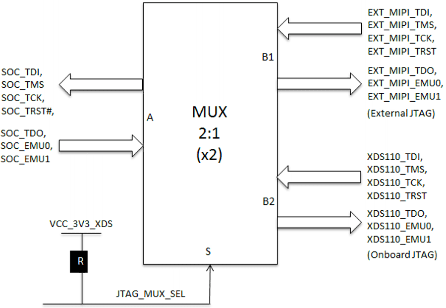
The Common processor board includes XDS110 class on board emulation through the micro B connector J3. It also has an option to support external emulation through MIPI 60 pin header. When an external emulator is connected, XDS110 emulation circuitry path will be disconnected automatically.
 Figure 4-39 JTAG Mux
| Condition | MUX_SEL | Function |
|---|---|---|
| XDS110 Powered via USB | HIGH | A<->B2 port [On Board EMU] |
| External Emulator attached | LOW | A<->B1 port [EXTERNAL EMU] |
As mentioned, the design includes the footprint for a MIPI 60-pin (J16) connector with connections for JTAG and trace capabilities. The trace pins are multiplexed with other functions (Multichannel Audio Serial Port (McASP0), McASP1, UART and MCAN) uses two on-board mux ICs (U10 and U14) on J7200 SoM to select the different functions. The mux is defaulted to the trace/McASP functions. The 1:3 mux ICs are controlled by bits of the I2C general-purpose input/output (GPIO) expander (I2C add: 0x21; I2C Inst:I2C0) on the J7200 SoM board.
Addition to the J7200 on-board, CPB uses two 1:3 on-board mux ICs (U44 & U121) to support audio and Trace functions. The mux is defaulted to MIPI 60pin connector. The 1:3 mux ICs are controlled by bits of the I2C GPIO expander2 (I2C add: 0x22; I2C Inst:I2C0) on Common Processor board. There is an option to set the state using the DIP switch SW3 Position 2.
| Pin No. | Signal | Pin No. | Signal |
|---|---|---|---|
| 1 | VSYS_IO_3V3 | 31 | TRC_DATA6 |
| 2 | MIPI_TMS | 32 | NC |
| 3 | MIPI_TCK | 33 | TRC_DATA7 |
| 4 | MIPI_TDO | 34 | NC |
| 5 | MIPI_TDI | 35 | TRC_DATA8 |
| 6 | MIPI_TGTRST# | 36 | NC |
| 7 | MIPI_RTCK | 37 | TRC_DATA9 |
| 8 | MIPI_TRST_PD (EXT_MIPI_TRST#) |
38 | EXT_MIPI_EMU0 |
| 9 | MIPI_nTRSTPU | 39 | TRC_DATA10 |
| 10 | NC | 40 | EXT_MIPI_EMU1 |
| 11 | NC | 41 | TRC_DATA11 |
| 12 | VSYS_IO_3V3 | 42 | NC |
| 13 | TRC_CLK | 43 | TRC_DATA12 |
| 14 | NC | 44 | NC |
| 15 | DGND | 45 | TRC_DATA13 |
| 16 | DGND | 46 | NC |
| 17 | TRC_CTL | 47 | TRC_DATA14 |
| 18 | TRC_DATA19 | 48 | NC |
| 19 | TRC_DATA0 | 49 | TRC_DATA15 |
| 20 | TRC_DATA20 | 50 | NC |
| 21 | TRC_DATA1 | 51 | TRC_DATA16 |
| 22 | TRC_DATA21 | 52 | NC |
| 23 | TRC_DATA2 | 53 | TRC_DATA17 |
| 24 | NC | 54 | NC |
| 25 | TRC_DATA3 | 55 | TRC_DATA18 |
| 26 | NC | 56 | NC |
| 27 | TRC_DATA4 | 57 | DGND |
| 28 | NC | 58 | JTAG_MUX_SEL |
| 29 | TRC_DATA5 | 59 | NC |
| 30 | NC | 60 | NC |
The EVM Common processor board Kit includes two JTAG converters, one is to convert MIPI 60 pin to TI14 pin JTAG emulator and the other one is to convert MIPI 60 pin to CTI20 pin JTAG.
Table 4-26 and Table 4-27 shows Pinouts of TI14 pin and CTI 20 pin JTAG converters.
| Pin No. | Signal | Pin No. | Signal |
|---|---|---|---|
| 1 | MIPI_20_TMS | 11 | MIPI_20_TCK |
| 2 | MIPI_20_TRST | 12 | DGND |
| 3 | MIPI_20_TDI | 13 | MIPI_20_EMU0 |
| 4 | MIPI_20_TDIS | 14 | MIPI_20_EMU1 |
| 5 | MIPI_20_VTREF | 15 | SYSRST# |
| 6 | NC (key) | 16 | DGND |
| 7 | MIPI_20_TDO | 17 | NC |
| 8 | 20PJTAG_DET | 18 | NC |
| 9 | MIPI_20_RTCK | 19 | NC |
| 10 | DGND | 20 | DGND |
| Pin No. | Signal | Pin No. | Signal |
|---|---|---|---|
| 1 | MIPI_14_TMS | 8 | 14PJTAG_DET |
| 2 | MIPI_14_TRST | 9 | MIPI_14_RTCK |
| 3 | MIPI_14_TDI | 10 | DGND |
| 4 | MIPI_14_TDIS | 11 | MIPI_14_TCK |
| 5 | MIPI_14_VTREF | 12 | DGND |
| 6 | NC (key) | 13 | MIPI_14_EMU0 |
| 7 | MIPI_14_TDO | 14 | MIPI_14_EMU1 |