SPRUIW7A October   2020  – February 2022


  1.   Trademarks
  2. 1Introduction
    1. 1.1 Key Features
    2. 1.2 Thermal Compliance
    3. 1.3 REACH Compliance
    4. 1.4 Electrostatic Discharge (ESD) Compliance
  3. 2J7200 EVM Overview
    1. 2.1 J7200 EVM Board Identification
    2. 2.2 J7200 SOM Component Identification
    3. 2.3 Jacinto7 Common Processor Component Identification
    4. 2.4 Quad Ethernet Components Identification
  4. 3EVM User Setup/Configuration
    1. 3.1 Power Requirements
    2. 3.2 Power ON Switch and Power LEDs
      1. 3.2.1 Over Voltage and Under Voltage Protection Circuit
      2. 3.2.2 Power Regulators and Power Status LEDs
    3. 3.3 EVM Reset/Interrupt Push Buttons
    4. 3.4 EVM DIP Switches
      1. 3.4.1 EVM Configuration DIP Switch
      2. 3.4.2 SOM Configuration DIP Switch
      3. 3.4.3 Boot Modes
      4. 3.4.4 Other Selection Switches
    5. 3.5 EVM UART/COM Port Mapping
  5. 4J7200 EVM Hardware Architecture
    1. 4.1  J7200 EVM Hardware Top Level Diagram
    2. 4.2  J7200 EVM Interface Mapping
    3. 4.3  I2C Address Mapping
    4. 4.4  GPIO Mapping
    5. 4.5  Power Supply
      1. 4.5.1 Power Sequencing
      2. 4.5.2 Voltage Supervisor
      3. 4.5.3 DDR I/O Voltage Selection
      4. 4.5.4 J7200 SoC SLEEP Logic Operation
      5. 4.5.5 J7200 SoC MCU Only Operation
      6. 4.5.6 J7200 SoC GPIO Retention Operation
      7. 4.5.7 J7200 SoC DDR Retention Operation
      8. 4.5.8 Power Monitoring
      9. 4.5.9 Power Test Points
    6. 4.6  Reset
    7. 4.7  Clock
      1. 4.7.1 Processor’s Primary Clock
      2. 4.7.2 Processor’s Secondary/SERDES Ref Clock
      3. 4.7.3 EVM Peripheral Ref Clock
    8. 4.8  Memory Interfaces
      1. 4.8.1 LPDDR4 Interface
      2. 4.8.2 OSPI Interface
      3. 4.8.3 MMC Interface
        1. 4.8.3.1 MMC0 - eMMC Interface
        2. 4.8.3.2 MMC1 – Micro SD Interface
      4. 4.8.4 Board ID EEPROM Interface
      5. 4.8.5 Boot EEPROM Interface
    9. 4.9  MCU Ethernet Interface
      1. 4.9.1 Gigabit Ethernet PHY Default Configuration
    10. 4.10 QSGMII Ethernet Interface
    11. 4.11 PCIe Interface
      1. 4.11.1 X2 Lane PCIe Interface
    12. 4.12 USB Interface
      1. 4.12.1 USB 3.1 Interface
      2. 4.12.2 USB 2.0 Interface
        1. 4.12.2.1 To PCIe Card Wi-Fi/BT
        2. 4.12.2.2 To Expansion Connector
      3. 4.12.3 USB 3.0 Micro AB Interface (Reserved Port)
    13. 4.13 Audio Interface
      1. 4.13.1 Line IN Port
      2. 4.13.2 MIC Input Port
      3. 4.13.3 Line Out Port
      4. 4.13.4 Head Phone Port
      5. 4.13.5 Port Mapping
    14. 4.14 CAN Interface
      1. 4.14.1 MCU CAN0
      2. 4.14.2 MCU CAN1
      3. 4.14.3 MAIN CAN3 (supports WAKE function)
      4. 4.14.4 MAIN CAN0
    15. 4.15 FPD Interface (Audio Deserializer)
    16. 4.16 I3C Interface
      1. 4.16.1 Gyroscope
      2. 4.16.2 I3C Header
    17. 4.17 ADC Interface
    18. 4.18 RTC Interface
    19. 4.19 Apple Authentication Header
      1. 4.19.1 Module Interface
    20. 4.20 JTAG Emulation
    21. 4.21 EVM Expansion Connectors
    22. 4.22 ENET Expansion Connector
      1. 4.22.1 Power Requirements
      2. 4.22.2 Clock
        1. 4.22.2.1 Main Clock
        2. 4.22.2.2 Optional Clock
      3. 4.22.3 Reset Signals
      4. 4.22.4 Ethernet Interface
        1. 4.22.4.1 Quad Port SGMII PHY Default Configuration
      5. 4.22.5 Board ID EEPROM Interface
  6. 5Functional Safety
  7. 6Revision History

OSPI Interface

The J7200 SOM has 512-Mbit OSPI memory device of part number S28HS512TGABHM010 connected to OSPI0 interface of J7200 processor. The OSPI interface supports single and double data rates with memory speed up to 166 MHz SDR and 200 MHz DDR.

J7200 SOM is xSPI compliant, specifically JEDEC eXpanded SPI (JESD251) compliant.

The SOM board also supports an option to include Hyper Flash + Hyper RAM Mfr. Part# S71KS512SC0, which is a 512Mb flash + 64Mb DRAM. 12-bit Active mux TS3DDR3812RUAR is provided to select either OSPI or HBMC interface. The selection of OSPI and hyper flash will be done by using a DIP (SW3) switch which is populated on the CP board. For more details, see Section 3.4.1.
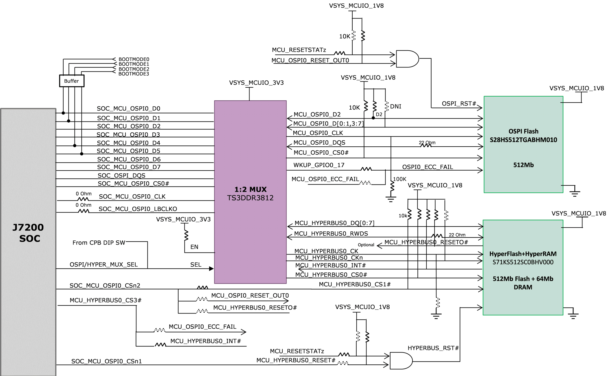
GUID-20200921-CA0I-TL3J-SZZQ-1QFMSSBX8N84-low.png Figure 4-12 J7200 SoM OSPI and Hyper Flash