SPRUIW7A October 2020 – February 2022
- Trademarks
- 1Introduction
- 2J7200 EVM Overview
- 3EVM User Setup/Configuration
-
4J7200 EVM Hardware Architecture
- 4.1 J7200 EVM Hardware Top Level Diagram
- 4.2 J7200 EVM Interface Mapping
- 4.3 I2C Address Mapping
- 4.4 GPIO Mapping
- 4.5 Power Supply
- 4.6 Reset
- 4.7 Clock
- 4.8 Memory Interfaces
- 4.9 MCU Ethernet Interface
- 4.10 QSGMII Ethernet Interface
- 4.11 PCIe Interface
- 4.12 USB Interface
- 4.13 Audio Interface
- 4.14 CAN Interface
- 4.15 FPD Interface (Audio Deserializer)
- 4.16 I3C Interface
- 4.17 ADC Interface
- 4.18 RTC Interface
- 4.19 Apple Authentication Header
- 4.20 JTAG Emulation
- 4.21 EVM Expansion Connectors
- 4.22 ENET Expansion Connector
- 5Functional Safety
- 6Revision History
3.4.3 Boot Modes
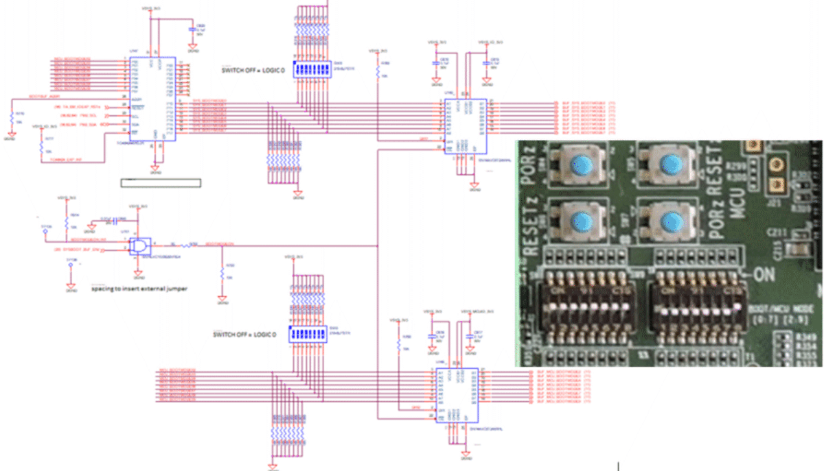
The boot mode for the processor is determined by a bank of DIP switches (SW8, SW9). All of the boot mode pins have week pull down resistors and a switch capable of connecting to a strong pull up resistor as shown in Figure 3-7. Note that the OFF setting provides a low logic level (‘0’) and an ON setting provides a high logic level (‘1’).
 Figure 3-7 BOOT Switches Provided on the
Processor Card
Figure 3-7 BOOT Switches Provided on the
Processor CardTable 3-7 and Table 3-8 provide the switch map to the boot mode functions. For specific settings for each boot interface, see the DRA821 Technical Reference Manual (SPRUIU2). The selectable boot interfaces supported on the EVM include: Octal-SPI, HyperFlash, SD-Card, eMMC, PCIe (as endpoint), CPSW, USB, UART, and EERPOM.
| Wakeup Boot Pin Map | ||||||||
|---|---|---|---|---|---|---|---|---|
| 0:1 (Fixed to ‘00’) |
2 (SW9.1= OFF) |
3 |
4 (SW9.3) |
5 (SW9.4) |
6 (SW9.5) |
7 (SW9.6) |
8 (SW9.7) |
9 (SW9.8) |
| PLL Configuration (Fixed to 19.2 MHz) | Primary Boot Mode A | MCU Only | Rsvd | Rsvd (not for boot use) | ||||
| Main Boot Mode Pin Map | |||||||
|---|---|---|---|---|---|---|---|
| 0 (SW8.1) |
1 (SW8.2) |
2 (SW8.3) |
(SW8.4 | 4 (SW8.5) |
5 (SW8.6) |
6 (SW8.7) |
7 (SW8.8) |
| Primary Boot Mode B | Backup Boot Mode | Primary Boot Mode Config | Backup Boot Mode Config | ||||
Below are a few common examples for EVM boot mode configuration. For the latest settings, it is still recommended to refer to the TRM.
| WKUP Bootmode | 2 | 3 | 4 | 5 | 6 | 7 | 8 | 9 |
|---|---|---|---|---|---|---|---|---|
| DIP SW9 | (SW9.1) | (SW9.2) | (SW9.3) | (SW9.4) | (SW9.5) | (SW9.6) | (SW9.7) | (SW9.8) |
| SD Boot (Default) | OFF | OFF | OFF | OFF | OFF | OFF | OFF | OFF |
| eMMC | OFF | ON | OFF | OFF | OFF | OFF | OFF | OFF |
| OSPI | OFF | ON | OFF | OFF | OFF | OFF | OFF | OFF |
| UART | OFF | ON | ON | ON | OFF | OFF | OFF | OFF |
| USB | OFF | OFF | ON | OFF | OFF | OFF | OFF | OFF |
| No Boot | OFF | ON | ON | ON | OFF | OFF | OFF | OFF |
| Main Bootmode | 0 | 1 | 2 | 3 | 4 | 5 | 6 | 7 |
|---|---|---|---|---|---|---|---|---|
| DIP SW8 | (SW8.1) | (SW8.2) | (SW8.3) | (SW8.4) | (SW8.5) | (SW8.6) | (SW8.7) | (SW8.8) |
| SD Boot (Default) | ON | OFF | OFF | OFF | OFF | OFF | ON | OFF |
| eMMC | ON | OFF | OFF | OFF | OFF | OFF | OFF | OFF |
| OSPI | OFF | OFF | OFF | OFF | OFF | ON | ON | OFF |
| UART | OFF | OFF | OFF | OFF | OFF | OFF | OFF | OFF |
| USB | ON | OFF | OFF | OFF | OFF | OFF | OFF | OFF |
| No Boot | ON | OFF | OFF | OFF | ON | OFF | OFF | OFF |