SWRA672 May 2020 AWR6843AOP , IWR6843AOP
4.2 Board Size Scaling
One of the ways to dissipate the heat is to use the board itself as a heat sink. The AoP mmWave sensor is built with FR4 PCB fabrication material designed to absorb the heat. In lot of the cases, it would satisfactorily handle the heat dissipation.
Copper traces/planes will have greater thermal conductivity than dielectric material of the PCB and readily conduct the heat through traces and planes in to larger section of the PCB. Hence, filled Cu material with plated through holes on the top/bottom and inner layers would help in spreading the heat to larger surface areas.
As a case study, various thermal simulations were performed to understand the effect of system thermal resistance on scaling of the board size at room temperature of 25 deg C. First mission side of the AOP board size is chosen and its thermal model is extracted and simulation results are extracted to different board size.
Table 1. Thermal Resistance Characteristics for 10% Duty Cycle for Various PCB Sizes
| 10% Duty PCB | PCB Area (mm2) | Device P (W) | Total P (W) | Tj (°C) | Case Temp (°C) | Board Temp (°C) | Psi-jc (°C/W) | Psi-jb (°C/W) | Effective Rja (°C/W) |
|---|---|---|---|---|---|---|---|---|---|
| Mission section PCB | 580 | 0.8808 | 1.2054 | 85.5 | 82.9 | 76.3 | 2.9 | 10.4 | 68.7 |
| Square PCB 30 | 900 | 0.8808 | 1.2054 | 73.1 | 70.6 | 64.5 | 2.9 | 9.8 | 54.6 |
| Square PCB 40 | 1600 | 0.8808 | 1.2054 | 62.0 | 59.5 | 53.3 | 2.9 | 9.8 | 42.0 |
| Square PCB 55 | 3025 | 0.8808 | 1.2054 | 53.9 | 51.4 | 45.2 | 2.9 | 9.9 | 32.8 |
| Square PCB 65 | 4225 | 0.8808 | 1.2054 | 51.0 | 48.4 | 42.3 | 2.9 | 9.8 | 29.5 |
Table 2. Thermal Resistance Characteristics for 25% Duty Cycle for Various PCB Sizes
| 25% Duty PCB | PCB Area (mm2) | Device P (W) | Total P (W) | Tj (°C) | Case Temp (°C) | Board Temp (°C) | Psi-jc (°C/W) | Psi-jb (°C/W) | Effective Rja (°C/W) |
|---|---|---|---|---|---|---|---|---|---|
| Mission section PCB | 580 | 1.2589 | 1.6838 | 105.1 | 102.1 | 92.7 | 2.4 | 9.8 | 63.6 |
| Square PCB 30 | 900 | 1.2589 | 1.6838 | 88.6 | 85.6 | 77.0 | 2.4 | 9.2 | 50.5 |
| Square PCB 40 | 1600 | 1.2589 | 1.6838 | 74.2 | 71.3 | 62.6 | 2.4 | 9.2 | 39.1 |
| Square PCB 55 | 3025 | 1.2589 | 1.6838 | 63.7 | 60.8 | 52.0 | 2.3 | 9.3 | 30.7 |
| Square PCB 65 | 4225 | 1.2589 | 1.6838 | 59.9 | 57.0 | 48.3 | 2.3 | 9.3 | 27.7 |
Table 3. Thermal Resistance Characteristics for 50% Duty Cycle for Various PCB Sizes
| 50% Duty PCB | PCB Area (mm2) | Device P (W) | Total P (W) | Tj (°C) | Case Temp (°C) | Board Temp (°C) | Psi-jc (°C/W) | Psi-jb (°C/W) | Effective Rja (°C/W) |
|---|---|---|---|---|---|---|---|---|---|
| Mission section PCB | 580 | 1.9 | 2.4949 | 134.3 | 130.0 | 116.4 | 2.3 | 9.4 | 57.5 |
| Square PCB 30 | 900 | 1.9 | 2.4949 | 113.6 | 109.3 | 96.4 | 2.3 | 9.1 | 46.6 |
| Square PCB 40 | 1600 | 1.9 | 2.4949 | 94.4 | 90.1 | 77.1 | 2.3 | 9.1 | 36.5 |
| Square PCB 55 | 3025 | 1.9 | 2.4949 | 80.3 | 76.0 | 62.9 | 2.3 | 9.1 | 29.1 |
| Square PCB 65 | 4225 | 1.9 | 2.4949 | 75.2 | 70.9 | 57.9 | 2.3 | 9.1 | 26.4 |
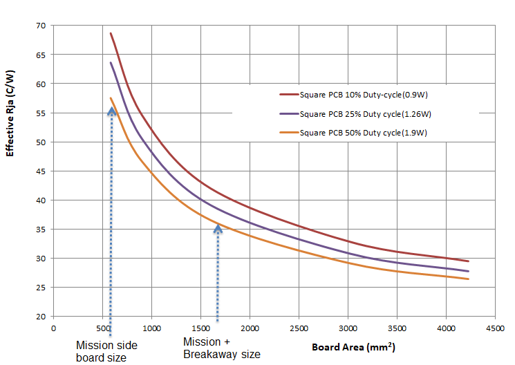
Figure 4 provides the summary of the effective thermal resistance junction to ambient for various board size and power dissipations.
 Figure 4. Effective Thermal Resistance vs Board Size for Various Duty Cycles
 It can be seen from the graph mission side alone PCB size (580) shows effective thermal resistance Rja close to 57-68 Deg C/W depending upon the duty cycle, Hence it has limited amount of power dissipation it can handle without using additional measures such as heatsink or enclosure to take the heat out from the board. However as PCB size increases it can be seen effective thermal resistance decreases beyond 3000 sq mm there is diminishing return from the board size increase in reducing effective thermal resistance.
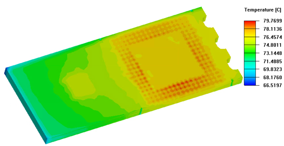
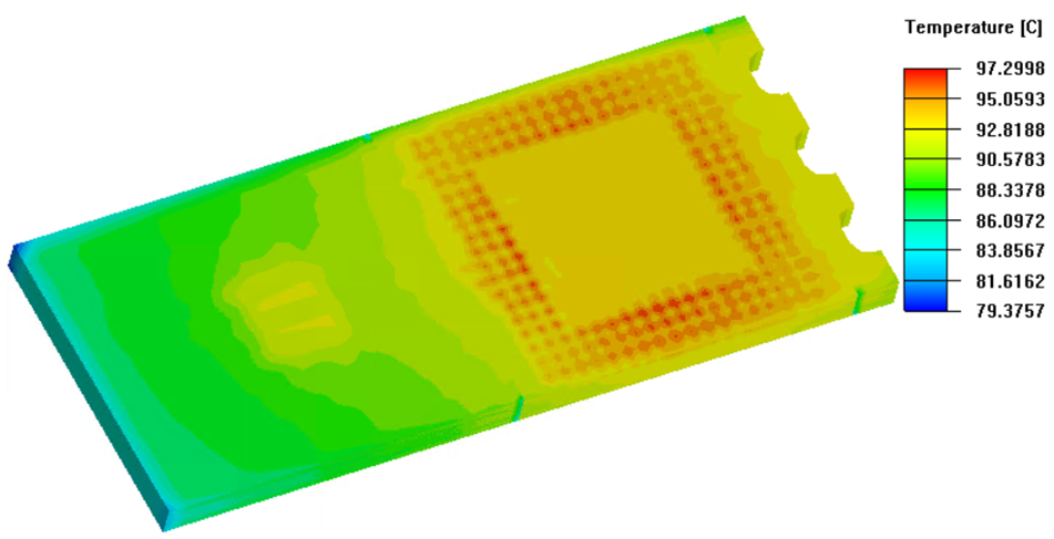
Figure 5 and Figure 6 shows the thermal simulation example done on the mission section of the EVM without any heatsink at 10% and 25% duty cycles, 25°C ambient temperatures.
 Figure 5. Thermal Simulation of Mission Side EVM With 10% Duty Cycle
  Figure 6. Thermal Simulation of Mission Side EVM With 25% Duty Cycle
 It can be seen from the simulation at 25% duty cycle and above, there is very little margin to reach maximum junction temperature. Hence it’s recommended to operate under 10% duty cycle without any heatsink or other thermal measures.