SWRA672 May 2020 AWR6843AOP , IWR6843AOP
5.1 Thermal via array
During the PCB design thermal vias plays important role in spreading the heat.
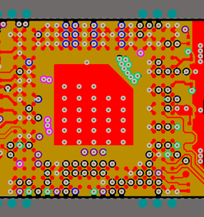
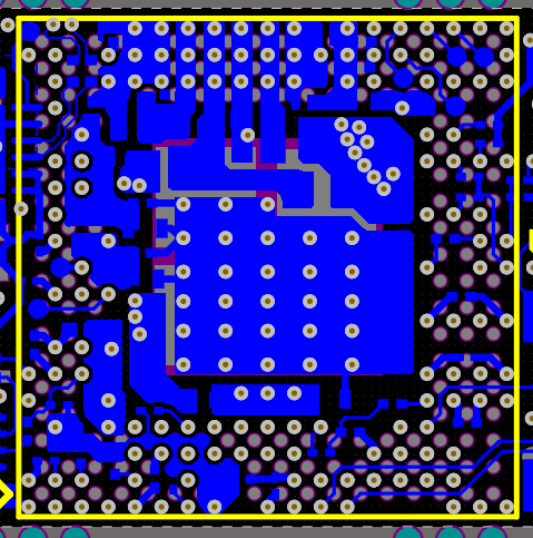
Plated through Via arrays are provided for planes and grounds in hotspot regions such as PMIC and underneath the sensors, these will help in spreading the heat to inner planes. Thicker plated through vias helps in better thermal conductivity, however excessive larger perforation of the PCB material also not recommended due to weakening power integrity.
Solid filled vias could be employed to conduct heat from thermal pads into ground planes; however, this will slightly increase the cost and complexity of PCB manufacturing process.
 Figure 19. Via Placement Under the BGA Top Side Layout Image
  Figure 20. Via Placement Under the BGA Bottom Side Layout Image
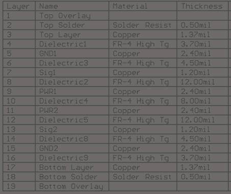
 Usage of large and multi-layer PCB boards helps to dissipate the heat; in this board 8 layers are used. Thicker copper clad is used in the inner ground/power planes. Thicker copper planes are better such as 2 oz copper in the inner plane and power layers. This also helps in improving the ground and power impedance along with better conductivity for the thermal. Care needs to be taken on the top, bottom routing layers aspect ratio of the traces need to be followed as per PCB fabricators recommendation. Sometimes too thick copper planes might restrict the minim trace width allowed in the design from high volume and reliable manufacturing perspective. Hence, this needs to be discussed with PCB fabricator before arriving right value. Also thicker copper will have slightly higher cost on the PCB manufacturing, hence right balance between cost and thermal design need to be considered.
 Figure 21. Layer Stack-Up and Copper Thickness