SWRA672 May 2020 AWR6843AOP , IWR6843AOP
5 PCB based thermal improvements
Proper PCB layout, focusing on thermal performance, results in lower die temperatures. Wide and thick power traces come with the ability to sink dissipated heat. This can be improved further on multi-layer PCB designs with vias to different planes. This results in reduced junction-to-ambient (RθJA) and junction-to-board (RθJB) thermal resistances and thereby reduces the device junction temperature, TJ. TI strongly recommends performing of a careful system-level 2D or full 3D dynamic thermal analysis at the beginning product design process, by using thermal modeling analysis software.
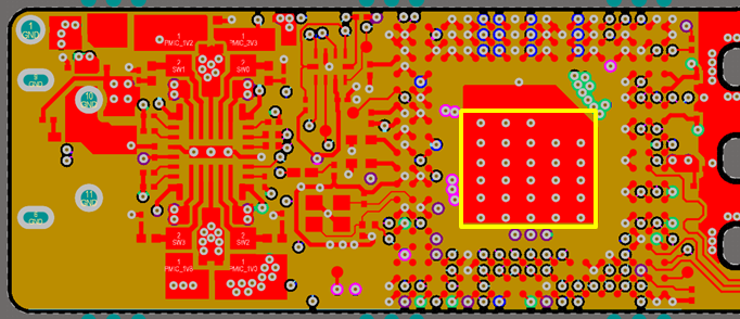
Figure 17 shows the top and bottom side of the AOP EVM, under the BGA area via array is placed which connects to ground layers in the board.
 Figure 17. Top Side of the PCB Layout Around the Sensor and PMIC Regions
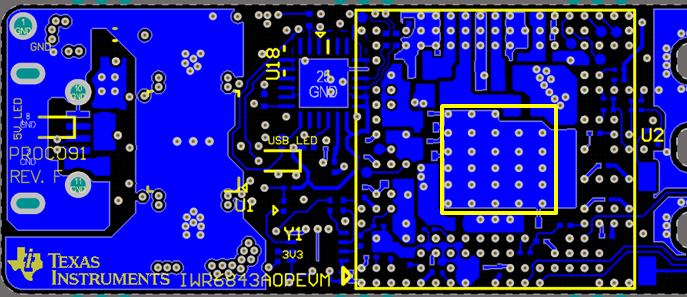
 On the bottom side of the board, below the BGA area solder mask could be opened. This would help in taking the heat out through the heatsink, as shown in Figure 18.
 Figure 18. Bottom Side of the PCB Layout Around the Sensor and PMIC Regions
 Provision for large GND plane/shape as allowable on the top, bottom and inner layers benefits distributing the heat laterally, especially right near the heat dissipating package would be beneficial for spreading the heat.