TIDUCL0 January   2017


  1. Description
  2. Resources
  3. Features
  4. Applications
  5. Design Images
  6. System Overview
    1. 6.1 System Description
    2. 6.2 Key System Specifications
    3. 6.3 Block Diagram
    4. 6.4 Highlighted Products
      1. 6.4.1 CSD88584Q5DC
      2. 6.4.2 DRV8323
      3. 6.4.3 MSP430F5132
      4. 6.4.4 TPS54061
      5. 6.4.5 LMT87
  7. System Design Theory
    1. 7.1 Power Stage Design—Battery Power Input to the Board
    2. 7.2 Power Stage Design—Three-Phase Inverter
      1. 7.2.1 Design Considerations in Paralleling MOSFETs
        1. 7.2.1.1 Conduction Phase
        2. 7.2.1.2 Switching Phase
      2. 7.2.2 Selecting the Sense Resistor
    3. 7.3 Power Stage Design—DRV8323 Gate Driver
      1. 7.3.1 Gate Drive Features of DRV8323
      2. 7.3.2 Current Shunt Amplifier in DRV8323
      3. 7.3.3 Protection Features in DRV8323
    4. 7.4 Power Stage Design—18-V to 3.3-V DC-DC Converter
    5. 7.5 Power Stage Design —Microcontroller MSP430
    6. 7.6 Power Stage Design—Hall Sensor Interface
    7. 7.7 Temperature Sensing
    8. 7.8 Power Stage Design—External Interface Options and Indications
      1. 7.8.1 Speed Control of Motor
      2. 7.8.2 Direction of Rotation—Digital Input
      3. 7.8.3 LED Indications
      4. 7.8.4 Signal Interface Connector for External Monitoring and Control
  8. Getting Started Hardware and Software
    1. 8.1 Hardware
      1. 8.1.1 Connector Configuration of TIDA-00774
      2. 8.1.2 Programming of MSP430
      3. 8.1.3 Procedure for Board Bring-up and Testing
    2. 8.2 Software
      1. 8.2.1 System Features
      2. 8.2.2 Customizing the Reference Code
        1. 8.2.2.1 PWM_PERIOD
        2. 8.2.2.2 MAX_DUTYCYCLE
        3. 8.2.2.3 MIN_DUTYCYCLE
        4. 8.2.2.4 ACCEL_RATE
        5. 8.2.2.5 Block_Rotor_Duration
      3. 8.2.3 Configuring the DRV8323 Registers (drv8323.c)
      4. 8.2.4 Initializing SPI Communication Between DRV8323 and MSP430 (drv8323.h)
      5. 8.2.5 Running Project in Code Composer Studio (CCS)
  9. Testing and Results
    1. 9.1 Test Setup
    2. 9.2 Test Data
      1. 9.2.1 Functional Tests
        1. 9.2.1.1 3.3-V Power Supply Generated by Step-Down Converter
        2. 9.2.1.2 Gate Drive Voltage Generated by Gate Driver
        3. 9.2.1.3 Dead Time From DRV8323
        4. 9.2.1.4 MOSFET Switching Waveforms
        5. 9.2.1.5 VGS Skew of Parallel FETs During Switching
      2. 9.2.2 Load Test
        1. 9.2.2.1 Load Test Without Heat Sink
        2. 9.2.2.2 Load Test With Heat Sink
        3. 9.2.2.3 Load Test With Heat Sink and Airflow
      3. 9.2.3 Inverter Efficiency Test
      4. 9.2.4 Thermal Rise at Different Power Levels
      5. 9.2.5 Inverter Current Sensing by VDS Monitoring
      6. 9.2.6 Overcurrent and Short-Circuit Protection Test
        1. 9.2.6.1 Cycle-by-Cycle Stall Current Protection by DRV8323 VDS Sensing
        2. 9.2.6.2 Stall Current Latch Protection by DRV8323 VDS Sensing
      7. 9.2.7 Testing for Peak Current Capability
  10. 10Design Files
    1. 10.1 Schematics
    2. 10.2 Bill of Materials
    3. 10.3 PCB Layout Recommendations
      1. 10.3.1 Layout Prints
    4. 10.4 Altium Project
    5. 10.5 Gerber Files
    6. 10.6 Assembly Drawings
  11. 11Software Files
  12. 12Related Documentation
    1. 12.1 Trademarks
  13. 13Terminology
  14. 14About the Author

Power Stage Design—Three-Phase Inverter

The three-phase inverter with two MOSFETs in parallel forms the power stage. Figure 3 shows one leg of the power stage, which consists of two power blocks. Each power block consists of two MOSFETs connected as a high-side and low-side FET. This device uses TI's patented stacked die technology in order to minimize parasitic inductances while offering a complete half bridge in a space saving thermally enhanced DualCool 5×6 mm package. With an exposed metal top, this power block device allows for simple heat sink applications to draw out heat through the top of the package and away from the PCB, for superior thermal performance at the higher currents demanded by many motor control applications.

The decoupling capacitors C18 and C19 are placed close across each power blocks to reduce the ringing in the supply lines because of the parasitic inductance added by the sense resistor and the power track.
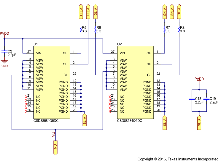
TIDA-00774 tida-00774-schematic-three-phase-mosfet-inverter.gifFigure 3. Schematic of Three-Phase MOSFET Inverter

NOTE

Connect the decoupling capacitors very near to the corresponding MOSFET legs for better decoupling. An improper layout or position of the decoupling capacitors can cause undesired VDS switching voltage spikes.

The DC bus current is measured using the current shunt resistors R13 and R15 mounted on the DC bus return path. The sensed currents are fed to the MCU through the current shunt amplifiers. The sense resistor is mainly used to measure the average battery current. The peak current in MOSFET is measured by monitoring the VDS.
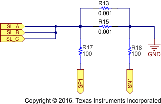
TIDA-00774 tida-00774-schematic-external-shunt-for-current-sensing.gifFigure 4. External Shunt for Current Sensing