SBAA383C January 2020 – January 2024 TLV320ADC3120 , TLV320ADC3140 , TLV320ADC5120 , TLV320ADC5140 , TLV320ADC6120 , TLV320ADC6140
3.1 ASI Configuration for Shared TDM
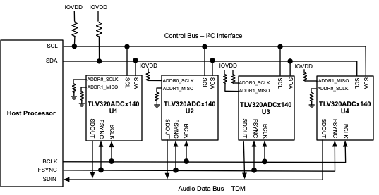
In Shared TDM bus configuration, the ASI buses of multiple TLV320ADCx140/PCMx140-Q1 devices are connected together into a single shared bus, as shown in Figure 3-2.
 Figure 3-2 TLV320ADCx140/PCMx140-Q1 Shared TDM Connection Diagram
To avoid multiple devices transmitting output data in the same slot, the TLV320ADCx140/PCMx140-Q1 supports mapping the input channels of a device to a programmable slot using the following registers:
- ASI_CH1 (Page 0x00, Register 0x0B), shown in Figure 3-3
- ASI_CH2 (Page 0x00, Register 0x0C), shown in Figure 3-4
- ASI_CH3 (Page 0x00, Register 0x0D), shown in Figure 3-5
- ASI_CH4 (Page 0x00, Register 0x0E), shown in Figure 3-6
This allows any channel to be mapped to any slot in any order. Furthermore, the TLV320ADCx140/PCMx140-Q1 also supports a secondary SDOUT output (SDOUT2) configured through the GPO_CFG0 register, bit field GPIO1_CFG with value of 0x03, as shown in Figure 3-14. This allows one or more devices outputting slots through two pins: primary output (SDOUT) and secondary output (SDOUT2). The ASI_CHx register bit field CHx_OUTPUT maps a slot to the primary (SDOUT) or secondary output (SDOUT2).
| 7 | 6 | 5 | 4 | 3 | 2 | 1 | 0 |
| Reserved | CH1_OUTPUT | CH1_SLOT[5:0] | |||||
| R-0h | R/W-0h | R/W-0h | |||||
| Bit | Field | Type | Reset | Description |
|---|---|---|---|---|
| 7 | Reserved | R | 0h | Reserved |
| 6 | CH1_OUTPUT | R/W | 0h | Channel 1 output line 0d = Channel 1 output is on the ASI primary output pin (SDOUT) 1d = Channel 1 output is on the ASI secondary output pin (GPIO1 or GPOx) |
| 5-0 | CH1_SLOT[5:0] | R/W | 0h | Channel 1 slot assignment 0d = TDM is slot 0 or I2S, LJ is left slot 0 1d = TDM is slot 1 or I2S, LJ is left slot 1 2d to 30d = Slot assigned as per configuration 31d = TDM is slot 31 or I2S, LJ is left slot 31 32d = TDM is slot 32 or I2S, LJ is right slot 0 33d = TDM is slot 33 or I2S, LJ is right slot 1 34d to 62d = Slot assigned as per configuration 63d = TDM is slot 63 or I2S, LJ is right slot 31 |
| 7 | 6 | 5 | 4 | 3 | 2 | 1 | 0 |
| Reserved | CH2_OUTPUT | CH2_SLOT[5:0] | |||||
| R-0h | R/W-0h | R/W-1h | |||||
| Bit | Field | Type | Reset | Description |
|---|---|---|---|---|
| 7 | Reserved | R | 0h | Reserved |
| 6 | CH2_OUTPUT | R/W | 0h | Channel 2 output line 0d = Channel 2 output is on the ASI primary output pin (SDOUT) 1d = Channel 2 output is on the ASI secondary output pin (GPIO1 or GPOx) |
| 5-0 | CH2_SLOT[5:0] | R/W | 1h | Channel 2 slot assignment 0d = TDM is slot 0 or I2S, LJ is left slot 0 1d = TDM is slot 1 or I2S, LJ is left slot 1 2d to 30d = Slot assigned as per configuration 31d = TDM is slot 31 or I2S, LJ is left slot 31 32d = TDM is slot 32 or I2S, LJ is right slot 0 33d = TDM is slot 33 or I2S, LJ is right slot 1 34d to 62d = Slot assigned as per configuration 63d = TDM is slot 63 or I2S, LJ is right slot 31 |
| 7 | 6 | 5 | 4 | 3 | 2 | 1 | 0 |
| Reserved | CH3_OUTPUT | CH3_SLOT[5:0] | |||||
| R-0h | R/W-0h | R/W-2h | |||||
| Bit | Field | Type | Reset | Description |
|---|---|---|---|---|
| 7 | Reserved | R | 0h | Reserved |
| 6 | CH3_OUTPUT | R/W | 0h | Channel 3 output line 0d = Channel 3 output is on the ASI primary output pin (SDOUT) 1d = Channel 3 output is on the ASI secondary output pin (GPIO1 or GPOx) |
| 5-0 | CH3_SLOT[5:0] | R/W | 2h | Channel 3 slot assignment 0d = TDM is slot 0 or I2S, LJ is left slot 0 1d = TDM is slot 1 or I2S, LJ is left slot 1 2d to 30d = Slot assigned as per configuration 31d = TDM is slot 31 or I2S, LJ is left slot 31 32d = TDM is slot 32 or I2S, LJ is right slot 0 33d = TDM is slot 33 or I2S, LJ is right slot 1 34d to 62d = Slot assigned as per configuration 63d = TDM is slot 63 or I2S, LJ is right slot 31 |
| 7 | 6 | 5 | 4 | 3 | 2 | 1 | 0 |
| Reserved | CH4_OUTPUT | CH4_SLOT[5:0] | |||||
| R-0h | R/W-0h | R/W-3h | |||||
| Bit | Field | Type | Reset | Description |
|---|---|---|---|---|
| 7 | Reserved | R | 0h | Reserved |
| 6 | CH4_OUTPUT | R/W | 0h | Channel 4 output line 0d = Channel 4 output is on the ASI primary output pin (SDOUT) 1d = Channel 4 output is on the ASI secondary output pin (GPIO1 or GPOx) |
| 5-0 | CH4_SLOT[5:0] | R/W | 3h | Channel 4 slot assignment 0d = TDM is slot 0 or I2S, LJ is left slot 0 1d = TDM is slot 1 or I2S, LJ is left slot 1 2d to 30d = Slot assigned as per configuration 31d = TDM is slot 31 or I2S, LJ is left slot 31 32d = TDM is slot 32 or I2S, LJ is right slot 0 33d = TDM is slot 33 or I2S, LJ is right slot 1 34d to 62d = Slot assigned as per configuration 63d = TDM is slot 63 or I2S, LJ is right slot 31 |
For the example of Figure 3-2, the following I2C script configures the input channels of U1–U4 into slots 0–15 for TLV320ADCx140/PCMx140-Q1, respectively. Note that slots are not assigned to the input channels of each device in sequence to show the flexibility of channel assignments to TDM slots:
w 98 0B 04  # Set U1 Ch1 mapped to slot 4 of SDOUT
w 98 0C 06  # Set U1 Ch2 mapped to slot 6 of SDOUT
w 98 0D 01  # Set U1 Ch3 mapped to slot 1 of SDOUT
w 98 0E 00  # Set U1 Ch4 mapped to slot 0 of SDOUT
w 9A 0B 03  # Set U2 Ch1 mapped to slot 3 of SDOUT
w 9A 0C 05  # Set U2 Ch2 mapped to slot 5 of SDOUT
w 9A 0D 02  # Set U2 Ch3 mapped to slot 2 of SDOUT
w 9A 0E 07  # Set U2 Ch4 mapped to slot 7 of SDOUT
w 9C 0B 08  # Set U3 Ch1 mapped to slot 8 of SDOUT
w 9C 0C 09  # Set U3 Ch2 mapped to slot 9 of SDOUT
w 9C 0D 0A  # Set U3 Ch3 mapped to slot 10 of SDOUT
w 9C 0E 0C  # Set U3 Ch4 mapped to slot 12 of SDOUT
w 9E 0B 0F  # Set U4 Ch1 mapped to slot 15 of SDOUT
w 9E 0C 0D  # Set U4 Ch1 mapped to slot 13 of SDOUT
w 9E 0D 0E  # Set U4 Ch1 mapped to slot 14 of SDOUT
w 9E 0E 0B  # Set U4 Ch1 mapped to slot 11 of SDOUT
This configuration requires that all the devices place their outputs in high-impedance mode, so another device can drive the bus. TLV320ADCx140/PCMx140-Q1 supports driving the output line low or placing it in high-impedance during unused bit clock cycles through the ASI_CFG0 register bit field TX_FILL, shown in Figure 3-7. Setting the TX_FILL places the primary (SDOUT) and secondary output line (SDOUT2) in high-impedance. Note the reset value configures SDOUT and SDOUT2 to drive low during unused bit clock cycles.
| 7 | 6 | 5 | 4 | 3 | 2 | 1 | 0 |
| ASI_FORMAT[1:0] | ASI_WLEN[1:0] | FSYNC_POL | BCLK_POL | TX_EDGE | TX_FILL | ||
| R/W-0h | R/W-3h | R/W-0h | R/W-0h | R/W-0h | R/W-0h | ||
| Bit | Field | Type | Reset | Description |
|---|---|---|---|---|
| 7-6 | ASI_FORMAT[1:0] | R/W | 0h | ASI protocol format 0d = TDM mode 1d = I2S mode 2d = LJ (left-justified) mode 3d = Reserved |
| 5-4 | ASI_WLEN[1:0] | R/W | 3h | ASI word or slot length 0d = 16 bits 1d = 20 bits 2d = 24 bits 3d = 32 bits |
| 3 | FSYNC_POL | R/W | 0h | ASI FSYNC polarity 0d = Default polarity as per standard protocol 1d = Inverted polarity with respect to standard protocol |
| 2 | BCLK_POL | R/W | 0h | ASI BCLK polarity 0d = Default polarity as per standard protocol 1d = Inverted polarity with respect to standard protocol |
| 1 | TX_EDGE | R/W | 0h | ASI data output (on the primary and secondary data pin) transmit edge 0d = Default edge as per the protocol configuration setting in bit 2 (BCLK_POL) 1d = Inverted following edge (half cycle delay) with respect to the default edge setting |
| 0 | TX_FILL | R/W | 0h | ASI data output (on the primary and secondary data pin) for any unused cycles 0d = Always transmit 0 for unused cycles 1d = Always use Hi-Z for unused cycles |
TLV320ADCx140/PCMx140-Q1 also supports tri-stating unused channels slots through the ASI_OUT_CH_EN register, as shown in Figure 3-8.
| 7 | 6 | 5 | 4 | 3 | 2 | 1 | 0 |
| ASI_OUT_CH1_EN | ASI_OUT_CH2_EN | ASI_OUT_CH3_EN | ASI_OUT_CH4_EN | ASI_OUT_CH5_EN | ASI_OUT_CH6_EN | ASI_OUT_CH7_EN | ASI_OUT_CH8_EN |
| R/W-0h | R/W-0h | R/W-0h | R/W-0h | R/W-0h | R/W-0h | R/W-0h | R/W-0h |
| Bit | Field | Type | Reset | Description |
|---|---|---|---|---|
| 7 | ASI_OUT_CH1_EN | R/W | 0h | ASI output channel 1 enable setting 0d = Channel 1 output slot is in a tri-state condition 1d = Channel 1 output slot is enabled |
| 6 | ASI_OUT_CH2_EN | R/W | 0h | ASI output channel 2 enable setting 0d = Channel 2 output slot is in a tri-state condition 1d = Channel 2 output slot is enabled |
| 5 | ASI_OUT_CH3_EN | R/W | 0h | ASI output channel 3 enable setting 0d = Channel 3 output slot is in a tri-state condition 1d = Channel 3 output slot is enabled |
| 4 | ASI_OUT_CH4_EN | R/W | 0h | ASI output channel 4 enable setting 0d = Channel 4 output slot is in a tri-state condition 1d = Channel 4 output slot is enabled |
| 3 | ASI_OUT_CH5_EN | R/W | 0h | ASI output channel 5 enable setting 0d = Channel 5 output slot is in a tri-state condition 1d = Channel 5 output slot is enabled |
| 2 | ASI_OUT_CH6_EN | R/W | 0h | ASI output channel 6 enable setting 0d = Channel 6 output slot is in a tri-state condition 1d = Channel 6 output slot is enabled |
| 1 | ASI_OUT_CH7_EN | R/W | 0h | ASI output channel 7 enable setting 0d = Channel 7 output slot is in a tri-state condition 1d = Channel 7 output slot is enabled |
| 0 | ASI_OUT_CH8_EN | R/W | 0h | ASI output channel 8 enable setting 0d = Channel 8 output slot is in a tri-state condition 1d = Channel 8 output slot is enabled |
To minimize power consumption by preventing pins from floating, the TLV320ADCx140/PCMx140-Q1 also supports enabling bus-keepers on SDOUT and SDOUT2 outputs. Register ASI_CFG1 controls the bus-keeper on the outputs through the TX_KEEPER bit field, as shown in Table 3-7. This register also controls the length of time SDOUT and SDOUT2 strongly drives the least significant bit (LSB) on the bus. This allows fine control so that two devices do not drive different signals on the same bus line at the same time, avoiding bus contention. For example, the LSB of U2 could be set to transmit on the first half of the bit clock cycle, while the MSB of U3 is driving without any offset. Moreover, selecting TX_KEEPER value of 0x2 or 0x3 adds robustness to the system by ensuring the LSB is latched properly by the host processor, since bus-keepers continue holding the bus with the last value driven. Note that this register also controls the number of bit clocks the most significant bit (MSB) is delayed.
| 7 | 6 | 5 | 4 | 3 | 2 | 1 | 0 |
| TX_LSB | TX_KEEPER[1:0] | TX_OFFSET[4:0] | |||||
| R/W-0h | R/W-0h | R/W-0h | |||||
| Bit | Field | Type | Reset | Description |
|---|---|---|---|---|
| 7 | TX_LSB | R/W | 0h | ASI data output (on the primary and secondary data pin) for LSB transmissions 0d = Transmit the LSB for a full cycle 1d = Transmit the LSB for the first half cycle and Hi-Z for the second half cycle |
| 6-5 | TX_KEEPER[1:0] | R/W | 0h | ASI data output (on the primary and secondary data pin) bus keeper 0d = Bus keeper is always disabled 1d = Bus keeper is always enabled 2d = Bus keeper is enabled during LSB transmissions only for one cycle 3d = Bus keeper is enabled during LSB transmissions only for one and half cycles |
| 4-0 | TX_OFFSET[4:0] | R/W | 0h | ASI data MSB slot 0 offset (on the primary and secondary data pin) 0d = ASI data MSB location has no offset and is as per standard protocol 1d = ASI data MSB location (TDM mode is slot 0 or I2S, LJ mode is the left and right slot 0) offset of one BCLK cycle with respect to standard protocol 2d = ASI data MSB location (TDM mode is slot 0 or I2S, LJ mode is the left and right slot 0) offset of two BCLK cycles with respect to standard protocol 3d to 30d = ASI data MSB location (TDM mode is slot 0 or I2S, LJ mode is the left and right slot 0) offset assigned as per configuration 31d = ASI data MSB location (TDM mode is slot 0 or I2S, LJ mode is the left and right slot 0) offset of 31 BCLK cycles with respect to standard protocol |
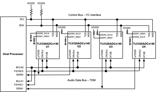
To support a greater number of slots than Equation 1 allows, multiple host processor TDM busses can split the TLV320ADCx140/PCMx140-Q1 devices connected, as shown in Figure 3-10. This connection method not only decreases the bit clock (BCLK) speed by half, but also reduces the load capacitance on the data lines SDIN1 and SDIN2 of the host processor.
 Figure 3-10 TLV320ADCx140/PCMx140-Q1 Shared Split TDM Connection Diagram
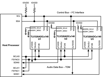
Another option is to use the secondary output to map slots of a single device to the primary and secondary output. For example, a system with 12 channels, 32-bit data words, and running with a 96-KHz sample rate requires a bit clock of 36.864 MHz (three devices * four channels/device * 32 bit words * 96 kHz), violating the maximum BCLK speed of 25 MHz. Dividing the 12 channels by assigning six channels to a primary bus and six channels to a secondary bus keeps the BCLK under 25 MHz. Since each device has four channels, one device has two channels assigned to the primary bus and two channels assigned to the secondary bus, as shown in Figure 3-11.
 Figure 3-11 TLV320ADCx140/PCMx140-Q1 Shared Split TDM With Primary and Secondary Bus Connection Diagram
For the example of Figure 3-11, the following I2C script configures U1, U2, and U3 for Shared TDM with primary and secondary bus.
w 98 0B 00  # Set U1 Ch1 mapped to slot 0 of SDOUT
w 98 0C 01  # Set U1 Ch2 mapped to slot 1 of SDOUT
w 98 0D 02  # Set U1 Ch3 mapped to slot 2 of SDOUT
w 98 0E 03  # Set U1 Ch4 mapped to slot 3 of SDOUT
w 9A 0B 04  # Set U2 Ch1 mapped to slot 4 of SDOUT
w 9A 0C 05  # Set U2 Ch2 mapped to slot 5 of SDOUT
w 9A 22 30  # Set U2 GPIO1 as SDOUT2
w 9A 0D 40  # Set U2 Ch3 mapped to slot 0 of SDOUT2
w 9A 0E 41  # Set U2 Ch4 mapped to slot 1 of SDOUT2
w 9C 22 30  # Set U3 GPIO1 as SDOUT2
w 9C 0B 42  # Set U3 Ch1 mapped to slot 2 of SDOUT2
w 9C 0C 43  # Set U3 Ch2 mapped to slot 3 of SDOUT2
w 9C 0D 44  # Set U3 Ch3 mapped to slot 4 of SDOUT2