SBAA383C January 2020 – January 2024 TLV320ADC3120 , TLV320ADC3140 , TLV320ADC5120 , TLV320ADC5140 , TLV320ADC6120 , TLV320ADC6140
1 Introduction
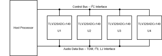
For TLV320ADx140 applications requiring more than four channels, multiple TLV320ADCx140/PCMx140-Q1 devices can share a common bus. For systems with up to 16 analog input channels or up to 32 digital microphone inputs, up to four TLV320ADCx140/PCMx140-Q1 devices can share a single control and audio data bus to minimize board routing area. TLV320ADCx140/PCMx140-Q1 supports a control bus using the I2C interface and an audio serial bus using a time-division multiplexed (TDM), Inter-IC Sound (I2S), or Left-justified (LJ) interface. Figure 1-1 shows a diagram of four TLV320ADCx140/PCMx140-Q1 devices sharing the control and audio data buses.
 Figure 1-1 Four TLV320ADCx140/PCMx140-Q1 Devices With Shared
Control and Audio Data Buses
Figure 1-1 Four TLV320ADCx140/PCMx140-Q1 Devices With Shared
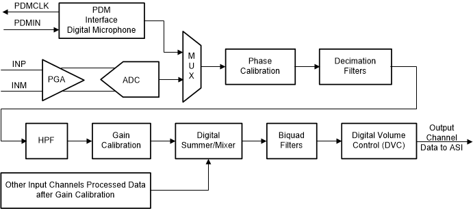
Control and Audio Data BusesEach channel of the TLV320ADCx140/PCMx140-Q1 device follows the signal chain shown in Figure 1-2. Each channel of the TLV320ADCx140/PCMx140-Q1 supports an analog differential or single-ended signal or a digital pulse density modulation (PDM) digital microphone. In TLV320ADCx140/PCMx140-Q1 device families, the analog input signal is amplified by a Programmable Gain Amplifier (PGA) and then converted by a high-performance ADC into a digital signal. The PGA gains the input signal to match the full scale of the ADC. The digital signal has a programmable phase calibration to adjust the phase delay of each channel in steps of one modulator clock cycle. This allows the system to match the phase across different channels. The phase-calibrated digital signal is then decimated through a set of linear phase filters or low-latency filters. DC offset is removed from the decimated signal through a Digital High Pass Filter (HPF) with three pre-set cutoff frequencies or a fully programmable cutoff frequency. Note that DC shifts are caused by mismatches in common-mode voltages. The output of the HPF is gain calibrated with 0.1 dB steps and summed with other channels. The gain calibration matches the gain across different channels, particularly if the channels have microphones with varying gain values. The output is then filtered by the Digital Biquad Filters and gained by the volume control.
 Figure 1-2 TLV320ADCx140/PCMx140-Q1 Channel Signal Chain
Processing Flow Chart
Figure 1-2 TLV320ADCx140/PCMx140-Q1 Channel Signal Chain
Processing Flow ChartThis application note concentrates on how to configure the TLV320ADCx140/PCMx140-Q1 to share a single control and audio data bus between the devices.