SBAU378A September 2021 – January 2022 ADS1148 , ADS1248
- Trademarks
- 1Introduction
- 2Getting Started With the ADS1x48EVM
-
3ADS1x48EVM Overview
- 3.1 Analog and Digital Power Supplies
- 3.2 Voltage Reference Options
- 3.3 Clock Options
- 3.4 Digital Interface
- 3.5
Analog Input Connections
- 3.5.1 Connecting a Thermocouple to J5 on the ADS1x48EVM
- 3.5.2 Connecting a Thermistor to J5 on the ADS1x48EVM
- 3.5.3
Connecting an RTD to J6 on the ADS1x48EVM
- 3.5.3.1 Connecting a 2-Wire RTD Using a Low-Side RREF to J6 on the ADS1x48EVM
- 3.5.3.2 Connecting a 2-Wire RTD Using a High-Side RREF to J6 on the ADS1x48EVM
- 3.5.3.3 Connecting a 3-Wire RTD Using One IDAC and a Low-Side RREF to J6 on the ADS1x48EVM
- 3.5.3.4 Connecting a 3-Wire RTD Using One IDAC and a High-Side RREF to J6 on the ADS1x48EVM
- 3.5.3.5 Connecting a 3-Wire RTD Using Two IDACs and a Low-Side RREF to J6 on the ADS1x48EVM
- 3.5.3.6 Connecting a 3-Wire RTD Using Two IDACs and a High-Side RREF to J6 on the ADS1x48EVM
- 3.5.3.7 Connecting a 4-Wire RTD Using a Low-Side RREF to J6 on the ADS1x48EVM
- 3.5.3.8 Connecting a 4-Wire RTD Using a High-Side RREF to J6 on the ADS1x48EVM
- 3.5.3.9 Summary of ADS1x48EVM RTD Configuration Settings
- 3.5.4 Connecting a General-Purpose Input to J5 on the ADS1x48EVM
- 4ADS1x48EVM GUI
- 5Bill of Materials, Printed Circuit Board Layout, and Schematic
- 6Revision History
3.4 Digital Interface
The ADS1x48 devices support the digital SPI and functional modes as detailed in the 24-bit ADS1248 data sheet or the 16-bit ADS1148 data sheet. As stated in Section 3.1, the PAMBoard operates at a 3.3-V logic level provided by the host computer and the ADS1x48EVM board uses this same 3.3-V logic level for DVDD.
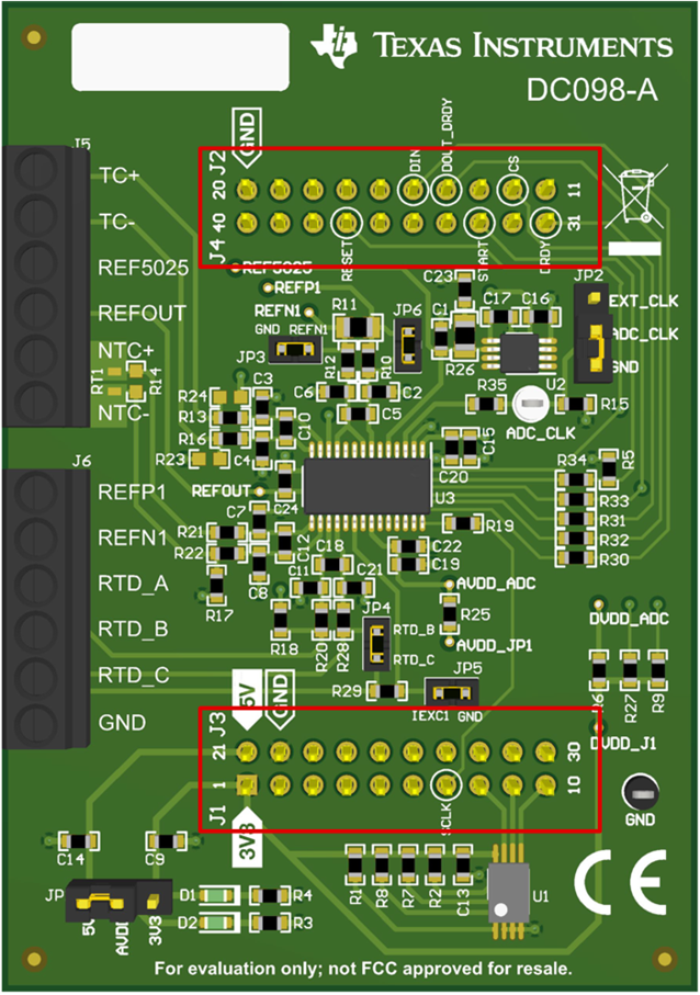
Digital interface connections from the ADS1x48EVM to the PAMBoard include power, I2C, SPI, and a GPIO connection used to trigger an interrupt at the end of conversion that signifies new data are available. The digital connections are highlighted in the silkscreen shown in Figure 3-5 and are described in detail in Table 3-2. Use these connection points for troubleshooting the SPI communication with a logic analyzer or to attach an external MCU to control the ADS1x48EVM without the PAMBoard.
 Figure 3-5 ADS1x48EVM-to-PAMBoard Connections
| Description | Connector | Connector | Description | Description | Connector | Connector | Connector |
|---|---|---|---|---|---|---|---|
| 3.3 V | J1:1 | J3:21 | 5 V | J4:40 | J2:20 | GND | |
| J1:2 | J3:22 | GND | J4:39 | J2:19 | |||
| J1:3 | J3:23 | J4:38 | J2:18 | ||||
| J1:4 | J3:24 | RESET | J4:37 | J2:17 | |||
| J1:5 | J3:25 | J4:36 | J2:16 | ||||
| J1:6 | J3:26 | J4:35 | J2:15 | DIN | |||
| SPI SCLK | J1:7 | J3:27 | J4:34 | J2:14 | DOUT/DRDY | ||
| J1:8 | J3:28 | START | J4:33 | J2:13 | |||
| I2C SCL | J1:9 | J3:29 | J4:32 | J2:12 | SPI CS | ||
| I2C SDA | J1:10 | J3:30 | DRDY | J4:31 | J2:11 | SPI CS |