SBAU378A September 2021 – January 2022 ADS1148 , ADS1248
- Trademarks
- 1Introduction
- 2Getting Started With the ADS1x48EVM
-
3ADS1x48EVM Overview
- 3.1 Analog and Digital Power Supplies
- 3.2 Voltage Reference Options
- 3.3 Clock Options
- 3.4 Digital Interface
- 3.5
Analog Input Connections
- 3.5.1 Connecting a Thermocouple to J5 on the ADS1x48EVM
- 3.5.2 Connecting a Thermistor to J5 on the ADS1x48EVM
- 3.5.3
Connecting an RTD to J6 on the ADS1x48EVM
- 3.5.3.1 Connecting a 2-Wire RTD Using a Low-Side RREF to J6 on the ADS1x48EVM
- 3.5.3.2 Connecting a 2-Wire RTD Using a High-Side RREF to J6 on the ADS1x48EVM
- 3.5.3.3 Connecting a 3-Wire RTD Using One IDAC and a Low-Side RREF to J6 on the ADS1x48EVM
- 3.5.3.4 Connecting a 3-Wire RTD Using One IDAC and a High-Side RREF to J6 on the ADS1x48EVM
- 3.5.3.5 Connecting a 3-Wire RTD Using Two IDACs and a Low-Side RREF to J6 on the ADS1x48EVM
- 3.5.3.6 Connecting a 3-Wire RTD Using Two IDACs and a High-Side RREF to J6 on the ADS1x48EVM
- 3.5.3.7 Connecting a 4-Wire RTD Using a Low-Side RREF to J6 on the ADS1x48EVM
- 3.5.3.8 Connecting a 4-Wire RTD Using a High-Side RREF to J6 on the ADS1x48EVM
- 3.5.3.9 Summary of ADS1x48EVM RTD Configuration Settings
- 3.5.4 Connecting a General-Purpose Input to J5 on the ADS1x48EVM
- 4ADS1x48EVM GUI
- 5Bill of Materials, Printed Circuit Board Layout, and Schematic
- 6Revision History
3.5.1 Connecting a Thermocouple to J5 on the ADS1x48EVM
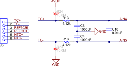
Connect an external thermocouple directly to the J5:1 and J5:2 inputs on the J5 terminal block, which represent the TC+ and TC– nets, respectively. The differential filter for this differential input pair has a cutoff frequency of 1.93 kHz. Additionally, each input has a common-mode filter with a cutoff frequency of 38.63 kHz. TC+ and TC– are connected through the filter resistors to two analog inputs (AIN4 and AIN5, respectively) on the ADS1x48. Figure 3-7 shows the portion of the ADS1x48EVM schematic with J5 and the thermocouple input structure.
 Figure 3-7 Thermocouple Input Structure on the ADS1x48EVM
Although thermocouples are self-powered, these components must be biased in order to avoid floating beyond the input range of the PGA integrated into the ADC. The ADS1x48EVM offers multiple ways to bias the thermocouple so that the output voltage can be successfully read by the ADC.
The first method uses pullup and pulldown resistors, which are labeled in Figure 3-7 as R24 and R23, respectively. These resistors are do not place (DNP) and therefore do not come installed on the EVM. To use the pullup and pulldown resistor method, install 1-MΩ to 10-MΩ resistors in the aforementioned locations. With these resistors installed, the thermocouple output voltage is centered at AVDD / 2, which puts the output voltage in the middle of the common-mode range of the PGA integrated into the ADS1x48. Additionally, using pullup and pulldown resistors enables continuous sensor break detection. If one of the thermocouple wires breaks, AIN4 is pulled to AVDD and AIN5 is pulled to GND, resulting in a full-scale input that can be detected in a separate firmware routine.
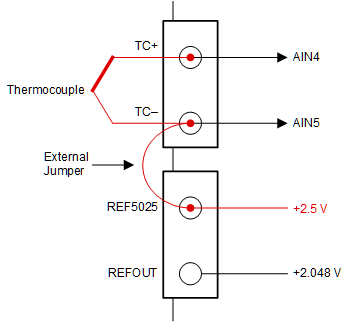
The second thermocouple-biasing method supported by the ADS1x48EVM uses one of the two reference voltage output pins to bias TC–. For example, Figure 3-8 shows that connecting an external jumper between the TC– input (J5:2) and the REF5025 output (J5:3) biases the thermocouple voltage to 2.5 V.
 Figure 3-8 Using REF5025 (input J5:3) to Bias a Thermocouple
If AVDD = 5 V in the configuration shown in Figure 3-8, the thermocouple output voltage is now centered in the middle of common-mode range of the PGA integrated in the ADS1x48. If AVDD is instead chosen to be 3.3 V, connect the external jumper between the REFOUT pin (J5:4) and the TC– input to bias the thermocouple output voltage to 2.048 V. Although this voltage is not equal to AVDD / 2 = 1.65 V, connecting TC– to REFOUT when AVDD = 3.3 V enables a wider PGA common-mode voltage swing compared to using the REF5025 output. An external bias voltage can also be directly connected to TC–.
One challenge with the biasing scheme in Figure 3-8 is that this configuration does not offer continuous wire-break detection. Instead, a separate diagnostic measurement can be made, or the pullup resistor (R24) in Figure 3-7 can be populated to help perform this function. To learn more about different thermocouple biasing schemes as well as how to measure these sensors with precision ADCs, see the A Basic Guide to Thermocouple Measurements application report. This document also discusses the need for cold junction compensation (CJC), which is used in conjunction with the thermocouple voltage to derive the measured temperature. The ADS1x48EVM includes provisions for a CJC measurement using a thermistor, which is discussed in more detail in the next section.
The steps for setting up a thermocouple measurement with the ADS1x48EVM are summarized below:
- Connect the sensor to the TC± terminals on J5
- Select a biasing scheme:
- For pullup and pulldown resistor biasing, populate R24 and R23, respectively
- For constant voltage biasing:
- Connect an external jumper between TC– and REF5025 or REFOUT
- Apply an external voltage to TC–
- Choose the ADC measurement channels to be MUX_SP[2:0] = AIN4 and MUX_SN[2:0] = AIN5
- Select the ADC reference source (REF5025, internal VREF, or external VREF)