SBAU378A September 2021 – January 2022 ADS1148 , ADS1248
- Trademarks
- 1Introduction
- 2Getting Started With the ADS1x48EVM
-
3ADS1x48EVM Overview
- 3.1 Analog and Digital Power Supplies
- 3.2 Voltage Reference Options
- 3.3 Clock Options
- 3.4 Digital Interface
- 3.5
Analog Input Connections
- 3.5.1 Connecting a Thermocouple to J5 on the ADS1x48EVM
- 3.5.2 Connecting a Thermistor to J5 on the ADS1x48EVM
- 3.5.3
Connecting an RTD to J6 on the ADS1x48EVM
- 3.5.3.1 Connecting a 2-Wire RTD Using a Low-Side RREF to J6 on the ADS1x48EVM
- 3.5.3.2 Connecting a 2-Wire RTD Using a High-Side RREF to J6 on the ADS1x48EVM
- 3.5.3.3 Connecting a 3-Wire RTD Using One IDAC and a Low-Side RREF to J6 on the ADS1x48EVM
- 3.5.3.4 Connecting a 3-Wire RTD Using One IDAC and a High-Side RREF to J6 on the ADS1x48EVM
- 3.5.3.5 Connecting a 3-Wire RTD Using Two IDACs and a Low-Side RREF to J6 on the ADS1x48EVM
- 3.5.3.6 Connecting a 3-Wire RTD Using Two IDACs and a High-Side RREF to J6 on the ADS1x48EVM
- 3.5.3.7 Connecting a 4-Wire RTD Using a Low-Side RREF to J6 on the ADS1x48EVM
- 3.5.3.8 Connecting a 4-Wire RTD Using a High-Side RREF to J6 on the ADS1x48EVM
- 3.5.3.9 Summary of ADS1x48EVM RTD Configuration Settings
- 3.5.4 Connecting a General-Purpose Input to J5 on the ADS1x48EVM
- 4ADS1x48EVM GUI
- 5Bill of Materials, Printed Circuit Board Layout, and Schematic
- 6Revision History
3.5.3.5 Connecting a 3-Wire RTD Using Two IDACs and a Low-Side RREF to J6 on the ADS1x48EVM
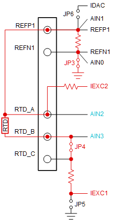
Figure 3-17 shows how to connect a 3-wire RTD using two IDACs and a low-side RREF configuration to J6.
 Figure 3-17 Connection Diagram for a
3-Wire RTD Using Two IDACs and a Low-Side RREF
Figure 3-17 Connection Diagram for a
3-Wire RTD Using Two IDACs and a Low-Side RREFFigure 3-17 also shows that for this RTD configuration, the RTD is connected to REFP1, RTD_A, and RTD_B. Additionally, jumpers JP3 and JP4 are connected whereas jumpers JP5 and JP6 are disconnected. Finally, the IEXC1 and IEXC2 current sources are enabled and the measurement is taken between AIN3 and AIN2. Table 3-5 summarizes the necessary connections and ADC configuration settings.