SBOA367B December 2019 – June 2022 TLV9001 , TLV9002 , TLV9004 , TLV9051 , TLV9052 , TLV9054 , TLV9061 , TLV9062 , TLV9064
- Designing for TLV90xxS operational amplifiers with shutdown
- Trademarks
- 1 Introduction
- 2 Shutdown Specifications
- 3 SHDN Pin Limits and Connections
- 4 Output Behavior During Enable and Shutdown
- 5 Enable Time and Shutdown Time Factors
- 6 Impact on Commonly Used Circuit Configurations
- 7 Advanced Circuit Functionality Using Amplifiers With Shutdown
- 8 Conclusion
- 9 References
- 10Revision History
 Figure 6-1 Inverting Amplifier
Circuit
Figure 6-1 Inverting Amplifier
CircuitThe fraction of the signal that is seen at the output will depend on the input signal frequency, the values of the resistors in the feedback network, the output load, the parasitic input capacitance and the output impedance of the amplifier when it is disabled. Consider an inverting amplifier circuit with a resistive load as an example. For this circuit, the voltage divider created by Ri+Rf and RLoad in parallel with RSHDN will set the maximum amount of signal from VIN that can be seen at VOUT. Note that RSHDN is typically very large, such that it can be ignored for this calculation. At high frequencies, the output impedance of the op amp itself will start to roll off, causing a low pass filter behavior at the output.
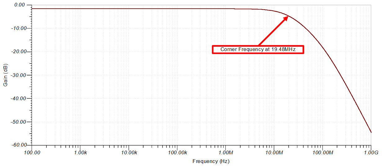
To see these effects simulated, consider an example of an inverting amplifier circuit in a gain of –1 V/V using the TLV9002S in shutdown mode. The circuit can be modeled using the setup in Figure 6-1. Set Ri and Rf to 1 kΩ and RLoad to 10 kΩ. From the TLV9002S data sheet specifications, CID is 1.5 pF, CCM is 5 pF, CSHDN is 2 pF, and RSHDN is 10 GΩ. Now an AC simulation is run to measure the response of the circuit. The result is shown in Figure 6-2.
 Figure 6-2 Inverting Amplifier AC
Response
Figure 6-2 Inverting Amplifier AC
ResponseThe simulation result shows a corner frequency of 19.48 MHz and a slope of –40 dB/dec at high frequencies due to the double pole. Notice that at low frequencies the input signal is attenuated by the ratio set by the sum of the feedback resistors and the load resistor. These form a DC path from input to output. Performing a voltage division calculation will yield an expected low frequency gain of 833 mV/V, or –1.58 dB. This demonstrates an important design consideration. This configuration may not significantly block or attenuate input signals from reaching the output while the amplifier is disabled. Thus, it is important to ensure that the output signal level during op amp shutdown is appropriate for the application.