SBOA367B December 2019 – June 2022 TLV9001 , TLV9002 , TLV9004 , TLV9051 , TLV9052 , TLV9054 , TLV9061 , TLV9062 , TLV9064
- Designing for TLV90xxS operational amplifiers with shutdown
- Trademarks
- 1 Introduction
- 2 Shutdown Specifications
- 3 SHDN Pin Limits and Connections
- 4 Output Behavior During Enable and Shutdown
- 5 Enable Time and Shutdown Time Factors
- 6 Impact on Commonly Used Circuit Configurations
- 7 Advanced Circuit Functionality Using Amplifiers With Shutdown
- 8 Conclusion
- 9 References
- 10Revision History
2 Shutdown Specifications
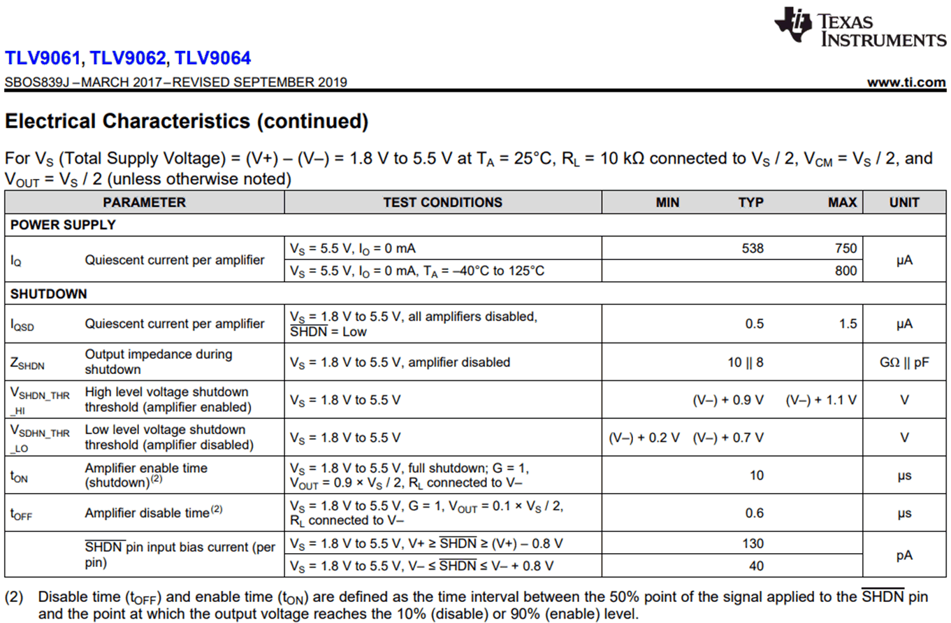
For the TLV90xxS family of products, the shutdown specifications are given in the “Electrical Characteristics” table of the device data sheet as shown for the TLV906xS in Figure 2-1 below. Not all TI op amps with shutdown functionality have the same information in their respective data sheets. However, most will specify the quiescent current when disabled, threshold voltages for the shutdown state, and enable/disable times. Definitions for the shutdown parameters follow in Table 2-1.
 Figure 2-1 TLV906xS Electrical Characteristics Table Shutdown Specifications
| Symbol | Parameter | Definition |
|---|---|---|
| IQSD | Quiescent current per amplifier | The current that a single channel consumes while it is disabled |
| ZSHDN | Output impedance during shutdown | The impedance looking back into the output pin of the amplifier while the amplifier has power at the rails but is in the disabled, or shutdown, state |
| VSHDN_THR_HI | High level voltage shutdown threshold (amplifier enabled) | The voltage level applied to the SHDN pin that enables the amplifier |
| VSHDN_THR_LO | Low level voltage shutdown threshold (amplifier disabled) | The voltage level applied to the SHDN pin that disables the amplifier |
| tON | Amplifier enable time (shutdown) | The time interval between the 50% point of the signal applied to the SHDN pin and the point at which the output voltage reaches 90% of the final output voltage |
| tOFF | Amplifier disable time | The time interval between the 50% point of the signal applied to the SHDN pin and the point at which the output voltage reaches 10% of the final output voltage |
| SHDN pin input bias current (per pin) | The amount of current that typically flows into the SHDN pin |
Some shutdown specifications are similar but different from specifications for amplifiers in normal operation. For example, the previously defined quiescent current during shutdown, IQSD, is similar to quiescent current, IQ. However, the test condition for the TLV906xS specifies that IQSD testing is done with all device channels disabled. As shown in Figure 2-1 above, the TLV906xS devices have a typical quiescent current of 0.5 µA while in the full shutdown state with all channels off. This is less than 0.1% of their typical IQ per channel of 538 µA while enabled.
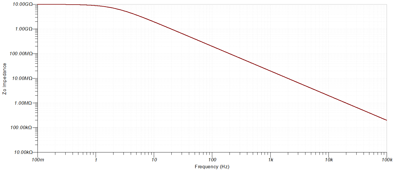
Similarly, ZSHDN is reminiscent of the amplifier's open-loop output impedance while the amplifier is enabled (ZO). ZSHDN is specified in Figure 2-1 as a parallel combination of a resistance (RSHDN) and a capacitance (CSHDN). When plotted over frequency, it resembles the curve shown in Figure 2-2. At DC, this impedance is equal to the resistance given in the specification table, 10 GΩ in this case. As the frequency increases, the capacitance begins to dominate the response and reduces the overall output impedance. For the TLV906xS devices, this impedance falls to 200 kΩ at 100 kHz.
 Figure 2-2 Output Impedance During Shutdown
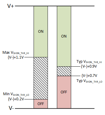
Finally, the shutdown devices feature threshold voltages, specified by VSHDN_THR_HI and VSHDN_THR_LO, that define the enable and disable regions via the SHDN pin. Between these voltages is an undefined state where the amplifier may be on, off, or some combination of the two states. The threshold voltages for the TLV90xxS devices are defined relative to the supply voltage. However, other devices may give absolute voltages for a specific supply. Figure 2-3 illustrates the SHDN pin regions using the threshold values from the TLV906xS data sheet with the grey striped area representing the undefined state. The left bar shows the minimum and maximum threshold values from the data sheet and the right bar shows the typical threshold values. To ensure proper operation, the minimum and maximum thresholds should be met during design.
 Figure 2-3 Shutdown Threshold Graphic