SBOA367B December 2019 – June 2022 TLV9001 , TLV9002 , TLV9004 , TLV9051 , TLV9052 , TLV9054 , TLV9061 , TLV9062 , TLV9064
- Designing for TLV90xxS operational amplifiers with shutdown
- Trademarks
- 1 Introduction
- 2 Shutdown Specifications
- 3 SHDN Pin Limits and Connections
- 4 Output Behavior During Enable and Shutdown
- 5 Enable Time and Shutdown Time Factors
- 6 Impact on Commonly Used Circuit Configurations
- 7 Advanced Circuit Functionality Using Amplifiers With Shutdown
- 8 Conclusion
- 9 References
- 10Revision History
4 Output Behavior During Enable and Shutdown
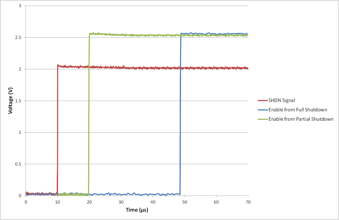
As mentioned above, there is a time delay from when a signal is applied to the SHDN pin to when the amplifier enters the desired state. This was defined previously as tON or tOFF. Figure 4-1 shows a typical enable transient response for the TLV9052S device, where the device is configured as specified in the "Shutdown" portion of the data sheet. Two enabling plots are shown: one from partial shutdown and one from full shutdown. A partial shutdown state means having one half the channels in the part enabled and the other half in shutdown. For full shutdown, all channels are disabled. Note that when the part comes out of partial shutdown, it has a significantly faster enable time. This occurs because some of the internal bias circuitry is left on to power the already enabled channel(s).
 Figure 4-1 TLV9052S Enable From Full
Shutdown and From Partial Shutdown
Figure 4-1 TLV9052S Enable From Full
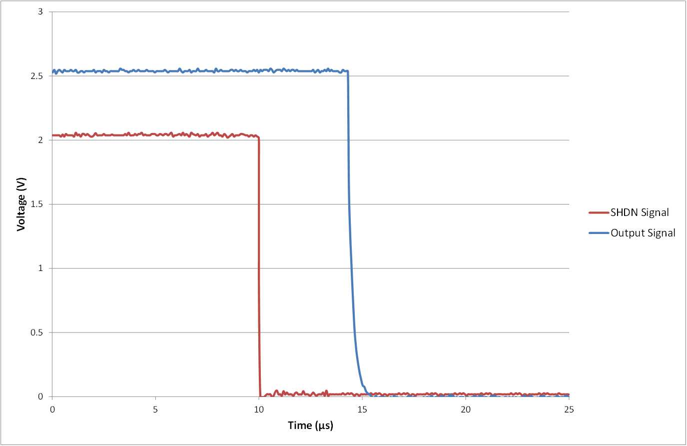
Shutdown and From Partial ShutdownSimilarly, Figure 4-2 shows channel 1 of the device being disabled when configured as outlined in the data sheet. Note that there is no distinction between disable times for putting the part into full shutdown versus partial shutdown. This is because each channel shuts down separately. Thus, only one shutdown time specification is required.
 Figure 4-2 TLV9052S Shutdown
Not all amplifiers enable in the same fashion. Some amplifiers have internal circuitry which allows for a controlled power up response. This circuit is called a power-on reset (POR) circuit and its purpose is to hold the output to a known state while the device enables. The POR function helps to prevent downstream logic from being inadvertently triggered.
For the TLV90xxS family of devices, the POR circuitry is non-functional when the device is powered off. The POR is activated when a startup current level is reached as the supply voltage is first applied. The POR circuit remains on while the amplifier is held in the shutdown state via the SHDN pin. Once the enable signal is sent to the SHDN pin, the POR circuitry holds the output until an internal biasing current reaches a threshold level. Then, the POR turns off and the amplifier is enabled.
In this manner, the TLV900xS, TLV905xS and TLV906xS devices can protect their outputs from unwanted behavior when the SHDN pin goes high to enable the device. Op amps that do not have POR circuitry may have a small glitch appear on the output when coming out of shutdown. This is more common in older parts.