SLAA457B September 2013 – October 2018 MSP430F5500 , MSP430F5501 , MSP430F5502 , MSP430F5503 , MSP430F5504 , MSP430F5505 , MSP430F5506 , MSP430F5507 , MSP430F5508 , MSP430F5509 , MSP430F5510 , MSP430F5513 , MSP430F5514 , MSP430F5515 , MSP430F5517 , MSP430F5519 , MSP430F5521 , MSP430F5522 , MSP430F5524 , MSP430F5525 , MSP430F5526 , MSP430F5527 , MSP430F5528 , MSP430F5529 , MSP430F5630 , MSP430F5631 , MSP430F5632 , MSP430F5633 , MSP430F5634 , MSP430F5635 , MSP430F5636 , MSP430F5637 , MSP430F5638 , MSP430F5658 , MSP430F5659 , MSP430F6630 , MSP430F6631 , MSP430F6632 , MSP430F6633 , MSP430F6634 , MSP430F6635 , MSP430F6636 , MSP430F6637 , MSP430F6638 , MSP430F6658 , MSP430F6659 , MSP430FG6425 , MSP430FG6426 , MSP430FG6625 , MSP430FG6626
4.2 Selecting a Power Configuration
The USB host provides 5-V power over the USB cable, called VBUS. A device can draw some or all of its power from VBUS. For devices that will be permanently "tethered" to the host, this can eliminate the need for a local power source.
For battery-powered devices – those that must be able to operate when detached from the host – VBUS power is still very valuable, because USB attachment can keep a device active for long periods of time, increasing the power requirements beyond what would be required otherwise. These devices can switch their power to VBUS while attached, to avoid draining the battery.
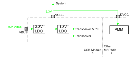
USB-equipped MSP430 devices have an integrated LDO that reduces 5-V VBUS to a nominal 3.3 V. This rail can be used to source:
- the USB module
- the MSP430 DVCC power rail (most MSP430 devices use a 1.8-V to 3.6-V DVCC rail)
- the rest of the board
The connection between the LDO and the USB module is internal. The rail is also made available on the VUSB pin. There is no internal connection between VUSB and DVCC; they are isolated from each other. This preserves flexibility for the engineer designer to arrange power in a way that is best for a given application.
The maximum current that can be drawn out of the VUSB pin, for use on DVCC and elsewhere on the board, is approximately 12 mA (see the device data sheet for specific parametric values). In some applications, this is sufficient for the entire system and can eliminate the need for any other LDO.
 Figure 9. Powering the Entire System From the Internal LDO
 Many other power arrangements are possible. For example:
- VUSB might be used only for USB, using a different source for DVCC or the rest of the system. If more than 12 mA is needed, this is a convenient approach.
- The internal 3.3-V LDO might be disabled, and 3.3 V can be driven into VUSB from an external source. Choosing an external LDO with ultra-low quiescent current can reduce current drain on VBUS during USB suspend.
- A switched approach can be employed: source DVCC and the system from a battery when USB is not attached but, upon attachment to a host, switch them to VBUS and VUSB
- USB battery charging can be employed, using a device such as TI's BQ24030.
VSSU is the ground for the USB module, including the transceiver and LDOs. The capacitors on VUSB and V18 should be kept as close as possible to VSSU, and VSSU should be tied to board ground.
For developers who want to source into VUSB from an external source, the Descriptor Tool includes a checkbox for this. If checked, it causes the USB API to keep the internal 3.3-V LDO disabled. However, you must still attach the VBUS signal from the USB cable to the VBUS pin, in the manner shown. The presence of 5 V on VBUS is the way in which USB devices determine whether a host is available; therefore, software needs this signal.