SLAAEC6A October 2023 – January 2024
- 1
- Description
- Get Started
- Features
- Applications
- 6
- 1Evaluation Module Overview
-
2Hardware
- 2.1 System Overview
- 2.2
Hardware Overview
- 2.2.1 AC-MB Settings
- 2.2.2 TAx5x1xQ1EVM-K Hardware Settings
- 2.2.3 Diagnostics Hardware Setup
- 2.2.4 GPIO1 Hardware Configurations
- 2.2.5 GPO1A Hardware Configurations
- 2.2.6 GPI1A Hardware Configurations
- 2.2.7 GPI2A Hardware Configurations
- 2.2.8 I2C Address Hardware Configurations
- 2.2.9 Audio Serial Interface Hardware Configurations
-
3Software
- 3.1 Software Description
- 3.2 PurePath Console 3 Installation
- 3.3
TAx5x1x-Q1 EVM GUI
- 3.3.1 Software Overview
- 3.3.2 Configuration View
- 3.3.3 End System Integration View
- 3.3.4 Register Map View
- 3.3.5 Preset Configuration
- 3.3.6 I2C Monitor View
- 3.4 Configuration Examples
- 4Hardware Design Files
- 5Additional Information
- 6Revision History
4.3 TAC541x-Q1 EVM Board Layout
The board layout consists of the top and bottom silkscreen, the top and bottom layer routings, the power planes, the two inner layout routings, and the ground planes. The layout applies to both the TAC5412-Q1 and TAC5411-Q1 EVM.
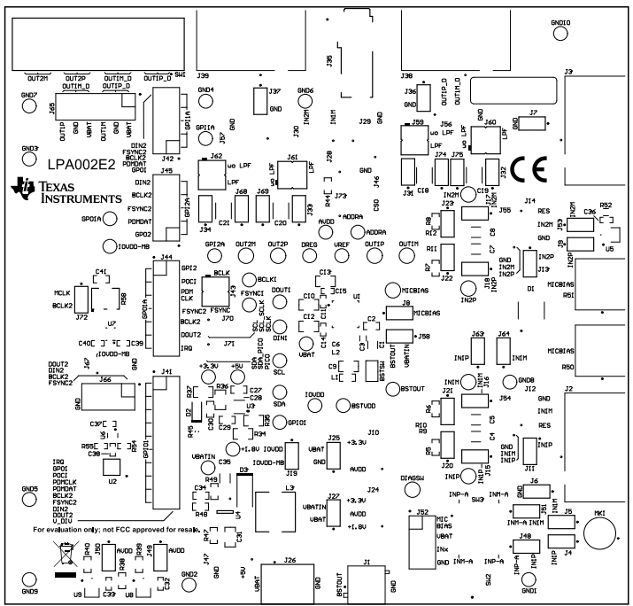 Figure 4-5 TAC541x-Q1 EVM Top Silkscreen
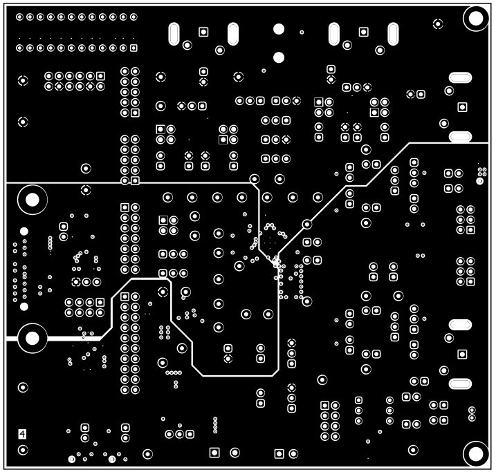 Figure 4-7 TAC541x-Q1 EVM Power Layer 1
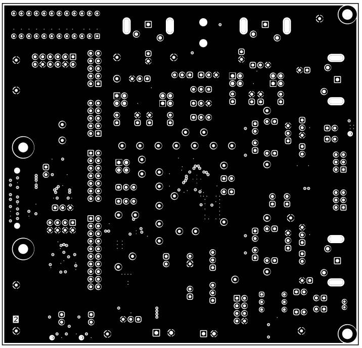 Figure 4-9 TAC541x-Q1 EVM Ground Layer 1
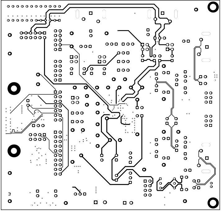 Figure 4-11 TAC541x-Q1 EVM Signal Layer 1
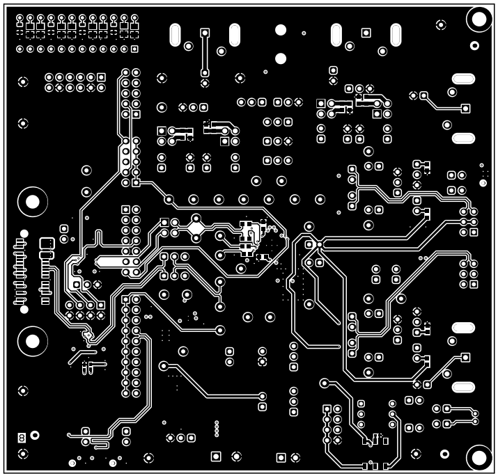 Figure 4-13 TAC541x-Q1 EVM Bottom Layer
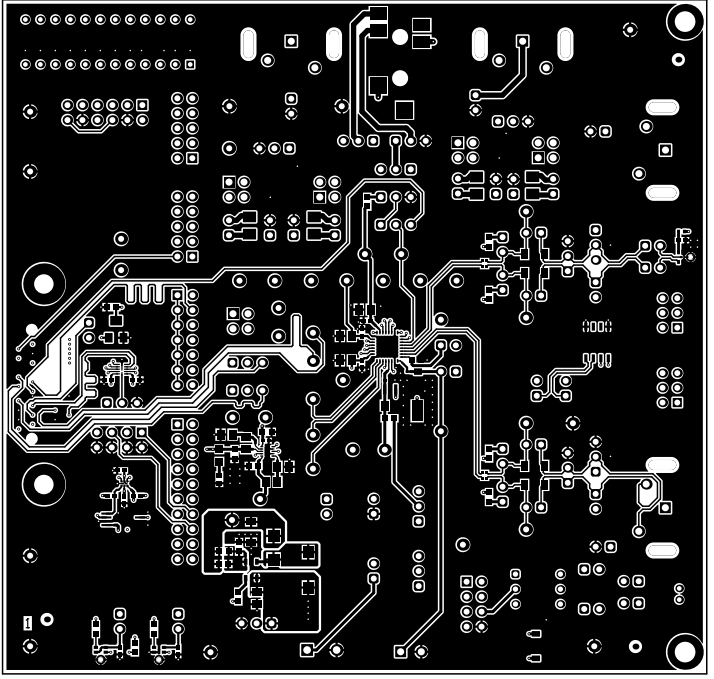 Figure 4-6 TAC541x-Q1 EVM Top Layer
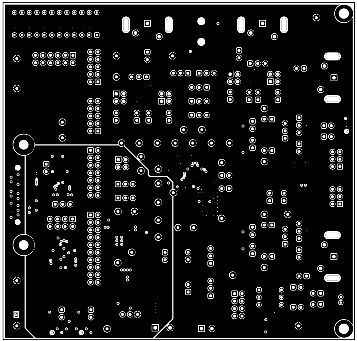 Figure 4-8 TAC541x-Q1 EVM Power Layer 2
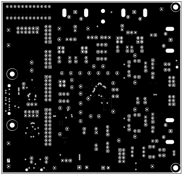 Figure 4-10 TAC541x-Q1 EVM Ground Layer 2
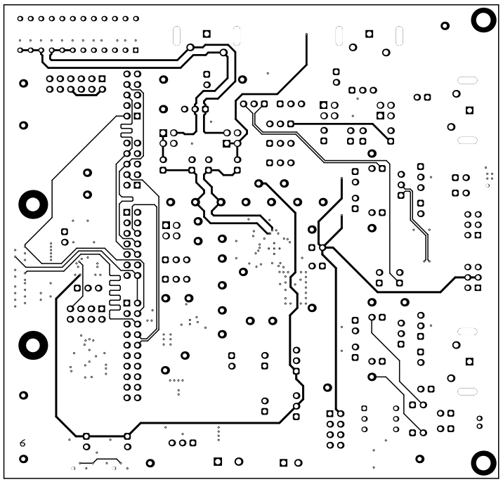 Figure 4-12 TAC541x-Q1 EVM Signal Layer 2
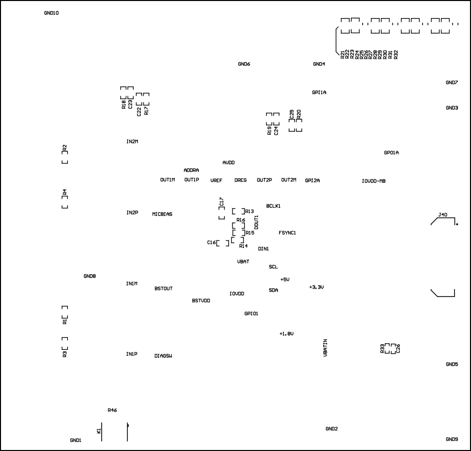 Figure 4-14 TAC541x-Q1 EVM Bottom Silkscreen