SLASEE5D January 2018 – January 2021 MSP430FR2422
PRODUCTION DATA
- 1 Features
- 2 Applications
- 3 Description
- 4 Functional Block Diagram
- 5 Revision History
- 6 Device Comparison
- 7 Terminal Configuration and Functions
-
8 Specifications
- 8.1 Absolute Maximum Ratings
- 8.2 ESD Ratings
- 8.3 Recommended Operating Conditions
- 8.4 Active Mode Supply Current Into VCC Excluding External Current
- 8.5 Active Mode Supply Current Per MHz
- 8.6 Low-Power Mode (LPM0) Supply Currents Into VCC Excluding External Current
- 8.7 Low-Power Mode (LPM3, LPM4) Supply Currents (Into VCC) Excluding External Current
- 8.8 Low-Power Mode (LPMx.5) Supply Currents (Into VCC) Excluding External Current
- 8.9 Typical Characteristics - Low-Power Mode Supply Currents
- 8.10 Typical Characteristics – Current Consumption Per Module
- 8.11 Thermal Resistance Characteristics
- 8.12 Timing and Switching Characteristics
-
9 Detailed Description
- 9.1 Overview
- 9.2 CPU
- 9.3 Operating Modes
- 9.4 Interrupt Vector Addresses
- 9.5 Bootloader (BSL)
- 9.6 JTAG Standard Interface
- 9.7 Spy-Bi-Wire Interface (SBW)
- 9.8 FRAM
- 9.9 Memory Protection
- 9.10
Peripherals
- 9.10.1 Power-Management Module (PMM)
- 9.10.2 Clock System (CS) and Clock Distribution
- 9.10.3 General-Purpose Input/Output Port (I/O)
- 9.10.4 Watchdog Timer (WDT)
- 9.10.5 System (SYS) Module
- 9.10.6 Cyclic Redundancy Check (CRC)
- 9.10.7 Enhanced Universal Serial Communication Interface (eUSCI_A0, eUSCI_B0)
- 9.10.8 Timers (Timer0_A3, Timer1_A3)
- 9.10.9 Hardware Multiplier (MPY)
- 9.10.10 Backup Memory (BAKMEM)
- 9.10.11 Real-Time Clock (RTC)
- 9.10.12 10-Bit Analog-to-Digital Converter (ADC)
- 9.10.13 Embedded Emulation Module (EEM)
- 9.11 Input/Output Diagrams
- 9.12 Device Descriptors
- 9.13 Memory
- 9.14 Identification
- 10Applications, Implementation, and Layout
- 11Device and Documentation Support
- 12Mechanical, Packaging, and Orderable Information
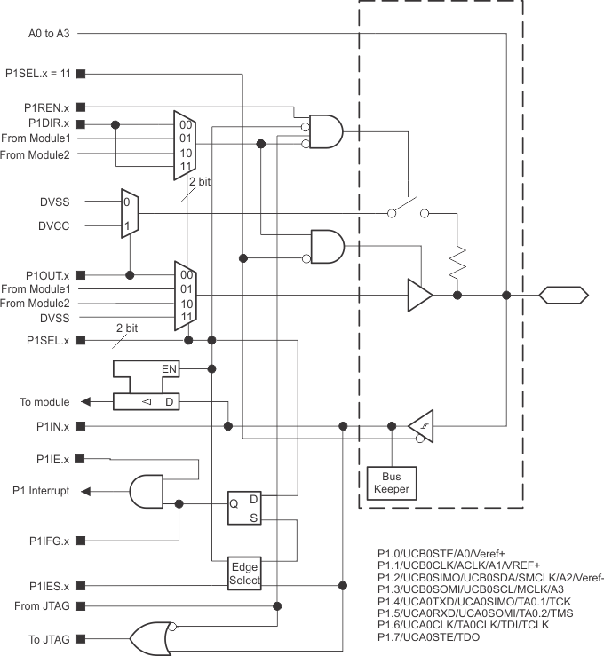
9.11.1 Port P1 (P1.0 to P1.7) Input/Output With Schmitt Trigger
Figure 9-3 shows the port diagram. Table 9-15 summarizes the selection of pin function.
 Figure 9-3 Port P1 (P1.0 to P1.7) Input/Output With Schmitt Trigger
Table 9-15 Port P1 (P1.0 to P1.7) Pin Functions
| PIN NAME (P1.x) | x | FUNCTION | CONTROL BITS AND SIGNALS(2) | |||
|---|---|---|---|---|---|---|
| P1DIR.x | P1SELx | ANALOG FUNCTION(1) | JTAG | |||
| P1.0/UCB0STE/A0/ Veref+ | 0 | P1.0 (I/O) | I: 0; O: 1 | 00 | 0 | 0 |
| UCB0STE | X | 01 | 0 | 0 | ||
| A0,Veref+ | X | ADCPCTLx = 1 (x = 0) from SYSCFG2 | N/A | |||
| P1.1/UCB0CLK/ACLK/ A1/VREF+ | 1 | P1.1 (I/O) | I: 0; O: 1 | 00 | 0 | 0 |
| UCB0CLK | X | 01 | 0 | 0 | ||
| ACLK | 1 | 10 | 0 | 0 | ||
| A1,VREF+ | X | ADCPCTLx = 1 (x = 1) from SYSCFG2 | N/A | |||
| P1.2/UCB0SIMO/ UCB0SDA/SMCLK/A2/ Veref- | 2 | P1.2 (I/O) | I: 0; O: 1 | 00 | 0 | 0 |
| UCB0SIMO/UCB0SDA | X | 01 | 0 | 0 | ||
| SMCLK | 1 | 10 | 0 | 0 | ||
| A2, Veref- | X | ADCPCTLx = 1 (x = 2) from SYSCFG2 | N/A | |||
| P1.3/UCB0SOMI/ UCB0SCL/MCLK/A3 | 3 | P1.3 (I/O) | I: 0; O: 1 | 00 | 0 | 0 |
| UCB0SOMI/UCB0SCL | X | 01 | 0 | 0 | ||
| MCLK | 1 | 10 | 0 | 0 | ||
| A3 | X | ADCPCTLx = 1 (x = 3) from SYSCFG2 | N/A | |||
| P1.4/UCA0TXD/ UCA0SIMO/TA0.1/TCK | 4 | P1.4 (I/O) | I: 0; O: 1 | 00 | 0 | Disabled |
| UCA0TXD/UCA0SIMO | X | 01 | 0 | Disabled | ||
| TA0.CCI1A | 0 | 10 | 0 | Disabled | ||
| TA0.1 | 1 | |||||
| JTAG TCK | X | X | X | TCK | ||
| P1.5/UCA0RXD/ UCA0SOMI/TA0.2/TMS | 5 | P1.5 (I/O) | I: 0; O: 1 | 00 | 0 | Disabled |
| UCA0RXD/UCA0SOMI | X | 01 | 0 | Disabled | ||
| TA0.CCI2A | 0 | 10 | 0 | Disabled | ||
| TA0.2 | 1 | |||||
| JTAG TMS | X | X | X | TMS | ||
| P1.6/UCA0CLK/ TA0CLK/TDI/TCLK | 6 | P1.6 (I/O) | I: 0; O: 1 | 00 | 0 | Disabled |
| UCA0CLK | X | 01 | 0 | Disabled | ||
| TA0CLK | 0 | 10 | 0 | Disabled | ||
| JTAG TDI/TCLK | X | X | X | TDI/TCLK | ||
| P1.7/UCA0STE/TDO | 7 | P1.7 (I/O) | I: 0; O: 1 | 00 | 0 | Disabled |
| UCA0STE | X | 01 | 0 | Disabled | ||
| JTAG TDO | X | X | X | TDO | ||
(1) Setting the bits disables both the output driver and input Schmitt trigger to prevent leakage when analog signals are applied.
(2) X = don't care