SLAU320AJ July   2010  – May 2021


  1.   Trademarks
  2. 1Introduction
    1. 1.1 About This Document
    2. 1.2 Organization of This Document
  3. 2Programming Using the JTAG Interface
    1. 2.1 Introduction
      1. 2.1.1 MSP430 JTAG Restrictions (Noncompliance With IEEE Std 1149.1)
      2. 2.1.2 TAP Controller State Machine
    2. 2.2 Interface and Instructions
      1. 2.2.1 JTAG Interface Signals
        1. 2.2.1.1 Pros and Cons of 2-Wire Spy-Bi-Wire and 4-Wire JTAG
        2. 2.2.1.2 4-Wire JTAG Interface
        3. 2.2.1.3 2-Wire Spy-Bi-Wire (SBW) JTAG Interface
      2. 2.2.2 JTAG Access Macros
        1. 2.2.2.1 Macros for 4-Wire JTAG Interface
          1. 2.2.2.1.1 IR_SHIFT (8-Bit Instruction)
          2. 2.2.2.1.2 DR_SHIFT16 (16-Bit Data)
          3. 2.2.2.1.3 DR_SHIFT20 (20-Bit Address) (Applies Only to MSP430X Devices)
          4. 2.2.2.1.4 MsDelay (Time)
          5. 2.2.2.1.5 SetTCLK
          6. 2.2.2.1.6 ClrTCLK
        2. 2.2.2.2 Macros for Spy-Bi-Wire (SBW) Interface
      3. 2.2.3 Spy-Bi-Wire (SBW) Timing and Control
        1. 2.2.3.1 Basic Timing
        2. 2.2.3.2 TMS Slot
          1. 2.2.3.2.1 TMSH Macro
          2. 2.2.3.2.2 TMSL Macro
          3. 2.2.3.2.3 TMSLDH Macro
        3. 2.2.3.3 TDI Slot
          1. 2.2.3.3.1 TDIH Macro
          2. 2.2.3.3.2 TDIL Macro
        4. 2.2.3.4 TDO Slot
          1. 2.2.3.4.1 TDO_RD Macro
          2. 2.2.3.4.2 TDOsbw Macro (No Read)
        5. 2.2.3.5 TCLK Handling in Spy-Bi-Wire (SBW) Mode
          1. 2.2.3.5.1 SetTCLK and ClrTCLK
          2. 2.2.3.5.2 TCLK Strobes
      4. 2.2.4 JTAG Communication Instructions
        1. 2.2.4.1 Controlling the Memory Address Bus (MAB)
          1. 2.2.4.1.1 IR_ADDR_16BIT
          2. 2.2.4.1.2 IR_ADDR_CAPTURE
        2. 2.2.4.2 Controlling the Memory Data Bus (MDB)
          1. 2.2.4.2.1 IR_DATA_TO_ADDR
          2. 2.2.4.2.2 IR_DATA_16BIT
          3. 2.2.4.2.3 IR_DATA_QUICK
          4. 2.2.4.2.4 IR_BYPASS
        3. 2.2.4.3 Controlling the CPU
          1. 2.2.4.3.1 IR_CNTRL_SIG_16BIT
          2. 2.2.4.3.2 IR_CNTRL_SIG_CAPTURE
          3. 2.2.4.3.3 IR_CNTRL_SIG_RELEASE
        4. 2.2.4.4 Memory Verification by Pseudo Signature Analysis (PSA)
          1. 2.2.4.4.1 IR_DATA_PSA
          2. 2.2.4.4.2 IR_SHIFT_OUT_PSA
        5. 2.2.4.5 JTAG Access Security Fuse Programming
          1. 2.2.4.5.1 IR_PREPARE_BLOW
          2. 2.2.4.5.2 IR_EX_BLOW
    3. 2.3 Memory Programming Control Sequences
      1. 2.3.1 Start-Up
        1. 2.3.1.1 Enable JTAG Access
        2. 2.3.1.2 Fuse Check and Reset of the JTAG State Machine (TAP Controller)
      2. 2.3.2 General Device (CPU) Control Functions
        1. 2.3.2.1 Function Reference for 1xx, 2xx, 4xx Families
          1. 2.3.2.1.1 Taking the CPU Under JTAG Control
          2. 2.3.2.1.2 Set CPU to Instruction-Fetch
          3. 2.3.2.1.3 Setting the Target CPU Program Counter (PC)
          4. 2.3.2.1.4 Controlled Stop or Start of the Target CPU
          5. 2.3.2.1.5 Resetting the CPU While Under JTAG Control
          6. 2.3.2.1.6 Release Device From JTAG Control
        2. 2.3.2.2 Function Reference for 5xx and 6xx Families
          1. 2.3.2.2.1 Taking the CPU Under JTAG Control
          2. 2.3.2.2.2 Setting the Target CPU Program Counter (PC)
          3. 2.3.2.2.3 Resetting the CPU While Under JTAG Control
          4. 2.3.2.2.4 Release Device From JTAG Control
          5. 2.3.2.2.5 74
      3. 2.3.3 Accessing Non-Flash Memory Locations With JTAG
        1. 2.3.3.1 Read Access
        2. 2.3.3.2 Write Access
        3. 2.3.3.3 Quick Access of Memory Arrays
          1. 2.3.3.3.1 Flow for Quick Read (All Memory Locations)
          2. 2.3.3.3.2 Flow for Quick Write
      4. 2.3.4 Programming the Flash Memory (Using the Onboard Flash Controller)
        1. 2.3.4.1 Function Reference for 1xx, 2xx, 4xx Families
        2. 2.3.4.2 Function Reference for 5xx and 6xx Families
      5. 2.3.5 Erasing the Flash Memory (Using the Onboard Flash Controller)
        1. 2.3.5.1 Function Reference for 1xx, 2xx, 4xx Families
          1. 2.3.5.1.1 Flow to Erase a Flash Memory Segment
          2. 2.3.5.1.2 Flow to Erase the Entire Flash Address Space (Mass Erase)
        2. 2.3.5.2 Function Reference for 5xx and 6xx Families
      6. 2.3.6 Reading From Flash Memory
      7. 2.3.7 Verifying the Target Memory
      8. 2.3.8 FRAM Memory Technology
        1. 2.3.8.1 Writing and Reading FRAM
        2. 2.3.8.2 Erasing FRAM
    4. 2.4 JTAG Access Protection
      1. 2.4.1 Burning the JTAG Fuse - Function Reference for 1xx, 2xx, 4xx Families
        1. 2.4.1.1 Standard 4-Wire JTAG
          1. 2.4.1.1.1 Fuse-Programming Voltage on TDI Pin (Dedicated JTAG Pin Devices Only)
          2. 2.4.1.1.2 Fuse-Programming Voltage On TEST Pin
        2. 2.4.1.2 Fuse-Programming Voltage Using SBW
      2. 2.4.2 Programming the JTAG Lock Key - Function Reference for 5xx, 6xx, and FRxx Families
        1. 2.4.2.1 Flash Memory Devices
        2. 2.4.2.2 FRAM Memory Devices
      3. 2.4.3 Testing for a Successfully Protected Device
      4. 2.4.4 Unlocking an FRAM Device in Protected and Secured Modes
        1. 2.4.4.1 FR5xx and FR6xx Devices
        2. 2.4.4.2 FR4xx and FR2xx Devices
      5. 2.4.5 Memory Protection Unit Handling
      6. 2.4.6 Intellectual Property Encapsulation (IPE)
      7. 2.4.7 FRAM Write Protection
    5. 2.5 JTAG Function Prototypes
      1. 2.5.1 Low-Level JTAG Functions
      2. 2.5.2 High-Level JTAG Routines
    6. 2.6 JTAG Features Across Device Families
    7. 2.7 References
  4. 3JTAG Programming Hardware and Software Implementation
    1. 3.1 Implementation History
    2. 3.2 Implementation Overview
    3. 3.3 Software Operation
    4. 3.4 Software Structure
      1. 3.4.1 Programmer Firmware
      2. 3.4.2 Target Code
        1. 3.4.2.1 Target Code Download for Replicator430, Replicator430X, and Replicator430Xv2
        2. 3.4.2.2 Target Code Download for Replicator430FR (FRAM)
    5. 3.5 Hardware Setup
      1. 3.5.1 Host Controller
      2. 3.5.2 Target Connection
      3. 3.5.3 Host Controller or Programmer Power Supply
      4. 3.5.4 Third-Party Support
  5. 4Errata and Revision Information
    1. 4.1 Known Issues
    2. 4.2 Revisions and Errata From Previous Documents
  6. 5Revision History

Target Connection

The target MSP430 device is connected to the host controller/programmer through the 14-pin connector labeled Target JTAG, which has the same standard signal assignment as all available MSP430 emulation tools with extra two pins that can be used for BSL connection. The programmable target device supply voltage of 2.1 V to 3.6 V with step 0.1 V is available on pin 2 of this connector, eliminating the need for an additional supply for the target system The required Spy-Bi-Wire or 4-wire JTAG and GND must be connected. (On devices requiring the TEST pin, the TEST signal also must be provided from the programmer to the target MSP430 device.) Host controller in the REP430F is supplied from the VCC = 3 V, while target device can be supplied with the VCC from 2.1 V to 3.6 V. To avoid a problem with I/O levels, the REP430V contains voltage level translators between target device and host controller. Voltage translators are supplied from the host controller VCC = 3 V from one side, and from the target's device VCC (provided on pin 2 of the target JTAG connector) from the other side. That allows supply the target device with the I/O levels exactly as required by the target device.)

To enable programming of all MSP430 flash-based devices including a JTAG access fuse, voltage translators are used and MOSFET switches are controlled by the host MSP430. MOSFET Q2 controls Vpp on devices with a TEST pin; Q1 connects Vpp to TDI on devices not requiring a TEST signal. U8 isolates the host controller from the target TEST pin while Vpp is connected to the target TEST input, while U6 isolates the host controller from the target TDI pin while Vpp is connected to the target TDI input. U7 connects the host TDI signal to the target TDO pin while the fuse is programmed (for devices without a TEST pin). The host controller program includes delays, which consider a MOSFET switching time of a maximum of 1 ms. Q1 and Q2 should have a Ron < 2 Ω to minimize voltage drop during fuse programming. While the fuse is being programmed, a maximum current flow of 100 mA is possible for approximately 2 µs into the TDI pin (or the TEST pin, depending on the target device).

Note:

An MSP430 flash programmer system designed for a specific MSP430 target device or a system not implementing fuse-blow functionality may require fewer relays or no relays at all. The programmer system described herein was developed with the intention that it can be used with any MSP430 flash- or FRAM-based device, across all families, including all memory access functionality, as well as fuse-blow capability.

Note:

Never unplug the JTAG cable during an active connection to the target device. Make sure that the debug or programming routine is completed before removing the JTAG connection.
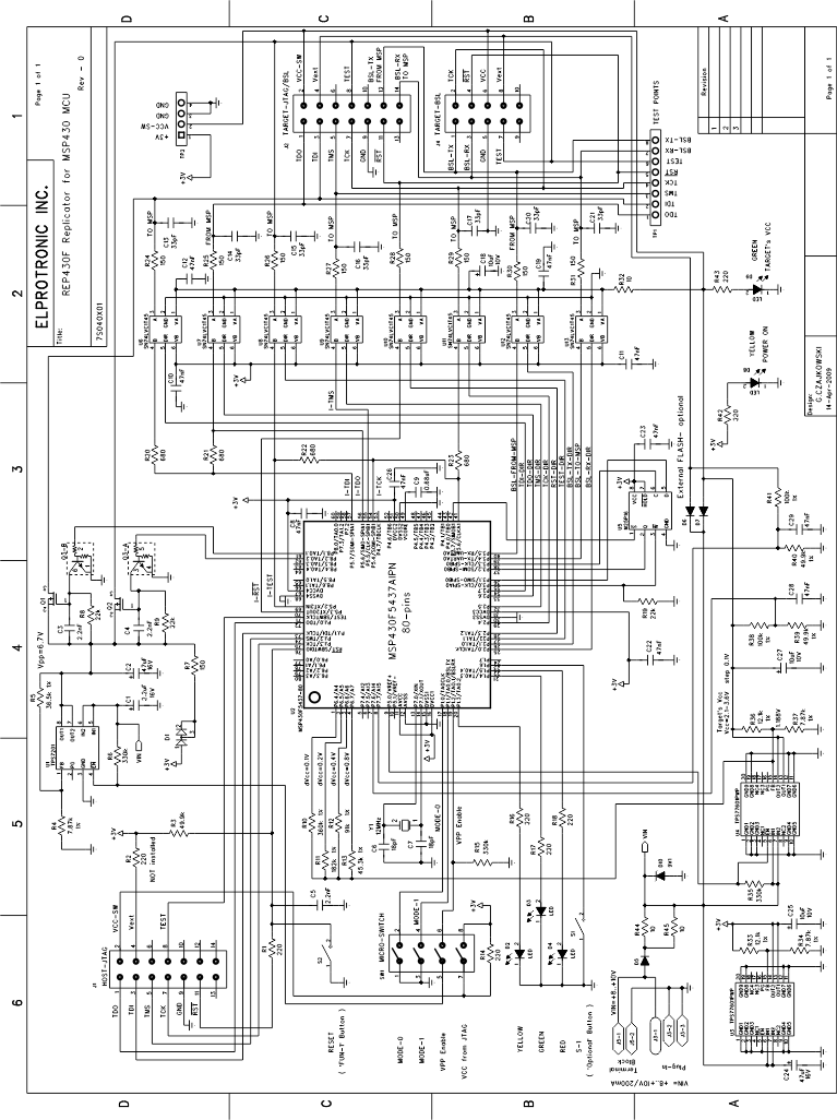
GUID-CFA37107-0CFA-4FD3-9806-A98923C17055-low.gifFigure 3-1 Replicator Application Schematic