SLLA272D February 2008 – May 2021
7 Failsafe
Failsafe operation is a receiver’s ability to assume a determined output state in the absence of an input signal.
Three possible causes can lead to the loss of signal (LOS):
- Open-circuit, caused by a wire break or by the disconnection of a transceiver from the bus
- Short-circuit, caused by an insulation fault connecting the wires of a differential pair to another
- Idle-bus, occurring when none of the bus drivers is active.
Because these conditions can cause conventional receivers to assume random output states when the input signal is zero, modern transceiver designs include biasing circuits for open-circuit, short-circuit, and idle-bus failsafe, that force the receiver output to a determined state, under an LOS condition.
A drawback of these failsafe designs is their worst-case noise margin of 10 mV only, thus requiring external failsafe circuitry to increase noise margin for applications in noisy environments.
An external failsafe circuit consists of a resistive voltage divider that generates sufficient differential bus voltage, to drive the receiver output into a determined state. To ensure sufficient noise margin, VAB must include the maximum differential noise measured in addition to the 200-mV receiver input threshold, VAB = 200 mV + VNoise.
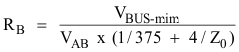
For a minimum bus voltage of 4.75 V, (5 V – 5%), VAB = 0.25 V, and Z0 = 120 W, RB yields 528 W. Inserting two 523-W resistors in series to RT establishes the failsafe circuit shown in Figure 7-1.
 Figure 7-1 External Idle-Bus Failsafe
Biasing
Figure 7-1 External Idle-Bus Failsafe
Biasing