SLLA472A March 2020 – February 2022 ISO5852S , ISO5852S-EP , ISO5852S-Q1 , LM2005 , LM2101 , LM2103 , LM2104 , LM2105 , LM25101 , LM27222 , LM2724A , LM5100A , LM5100B , LM5100C , LM5101 , LM5101A , LM5101B , LM5101C , LM5102 , LM5104 , LM5105 , LM5106 , LM5107 , LM5108 , LM5109 , LM5109A , LM5109B , LM5109B-Q1 , LM5113-Q1 , LMG1205 , LMG1210 , SM72295 , SM74104 , TPS28225 , TPS28225-Q1 , TPS28226 , TPS2832 , TPS2836 , TPS2837 , UC2950 , UCC27200 , UCC27200-Q1 , UCC27200A , UCC27201 , UCC27201A , UCC27201A-DIE , UCC27201A-Q1 , UCC27211 , UCC27211A , UCC27211A-Q1 , UCC27212 , UCC27212A-Q1 , UCC27222 , UCC27282 , UCC27282-Q1 , UCC27284 , UCC27284-Q1 , UCC27288 , UCC27289 , UCC27301A , UCC27301A-Q1 , UCC27311A , UCC27311A-Q1 , UCC27710 , UCC27712 , UCC27712-Q1 , UCC27714 , UCC27734 , UCC27734-Q1 , UCC27735 , UCC27735-Q1 , UCC27834 , UCC27834-Q1 , UCC27884 , UCC27884-Q1
3 Current Boost With Saturated MOSFET Totem Pole Stage
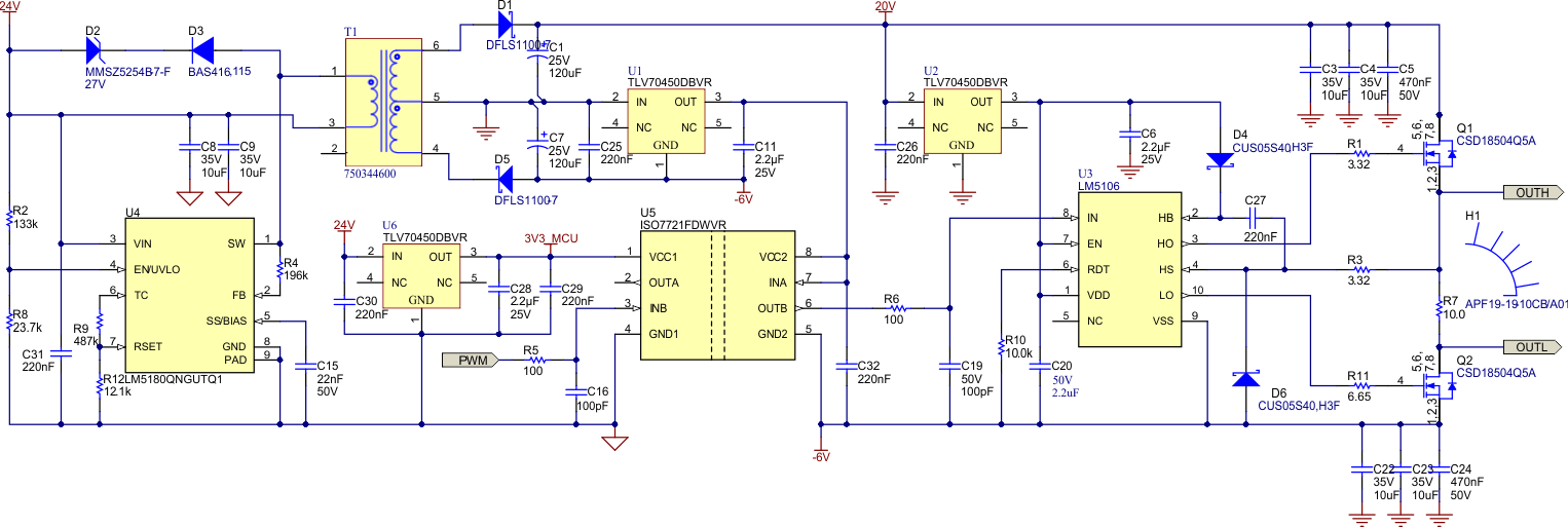
An alternate scheme for drive current boosting is given in Figure 3-1. Two N-channel MOSFETs are used as current boosting devices. As they are operated as saturated switches, the drive current is only limited by the on-time resistance and hence can achieve much higher current levels.
 Figure 3-1 High-Current Gate Driver Using
LM5106 and MOSFETs
Figure 3-1 High-Current Gate Driver Using
LM5106 and MOSFETsIn this circuit, signal isolation is provided by a digital isolator (ISO7721). To drive the driver MOSFETs, a low-voltage half-bridge driver IC (LM5106) is used. The power supply is the same as the previous circuit. However, a couple more LDOs are required to power the secondary side of the digital isolator and the half-bridge driver. The secondary side of the digital isolator is referred to the –6-V negative drive supply. So to power this side, a 5-V supply referred to this level is needed. This is provided by a 5-V LDO connected to the secondary return. For the gate-drive voltage for the driver MOSFETs (and the half bridge driver), a voltage of around 10 V (referred to the negative drive supply) is needed. This is generated by another 5-V LDO referred to the secondary return. This gives a total of 11 V (5 V from the LDO and 6 V from the negative drive supply) referred to as the negative drive supply.
For half-bridge drivers, typically two PWMs are required – the main PWM for the upper MOSFET and a complementary PWM for the lower MOSFET. However, the LM5106 half-bridge driver can generate the complementary signal internally with a dead-time determined by a programming resistor. This saves the need to have the complementary signal generated by the MCU. However, the half-bridge driver will need a level-shifted drive voltage to address the upper MOSFET. In this circuit, this voltage is provided by a bootstrap circuit comprising of D4, C27 , and R3 under the assumption that there is sufficient on-time for the lower MOSFET to charge. With the component values used in this circuit, the typical charging time is under 1 µs. That means, for PWM inputs with less than 1-µs off-time, the bootstrap capacitor might not be able to charge to the full supply voltage. Also, for low PWM frequencies (below a few 100 Hz), the bootstrap capacitor will not be able to hold the charge for the entire cycle. If such conditions are expected to be present, it is recommended to use an additional isolated supply to power the high-side – this can easily be generated by adding one more winding on the flyback power supply used. This will allow even 100% duty cycle operation.
The upper-side MOSFET is switched in accordance with the PWM input, while the lower MOSFET is switched based on the complementary of the PWM input resulting in output drive with the same polarity as the input PWM. As the drive current can be as high as 100 A, sufficient decoupling is required on the positive and negative drive-supply rails. If needed, additional capacitors can be added externally. This high peak current-drive capability is not required for most power devices, but by utilizing FETs of this power level, thermal dissipation can be greatly reduced when driving with peak currents of 20 A or higher. The peak current can be limited by using the external gate resistor since too high a peak current can result in undesirable ringing at the gate and uncontrolled slew rates of the power switch.