SLLA472A March 2020 – February 2022 ISO5852S , ISO5852S-EP , ISO5852S-Q1 , LM5106 , UCC27201A
5 Performance Results
Drive current: driving a total load of around 1 µF. Magenta – drive current, Green – drive voltage.
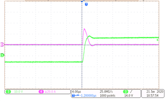 Figure 5-1 Drive-Current Waveform (Board 1)
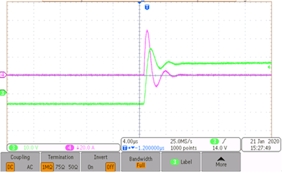 Figure 5-2 Drive-Current Waveform (Board 2)
Board 1 gives about 30-A drive current and Board 2 is able to give above 50 A.
Board 1 propagation delay: driving a total load of 470 nF. Magenta – PWM input, Green – drive voltage.
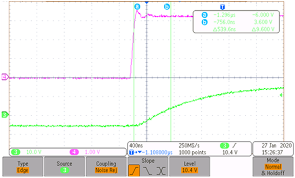
 Figure 5-4 Board 1 Propagation Delay Start of Input to Start of Output
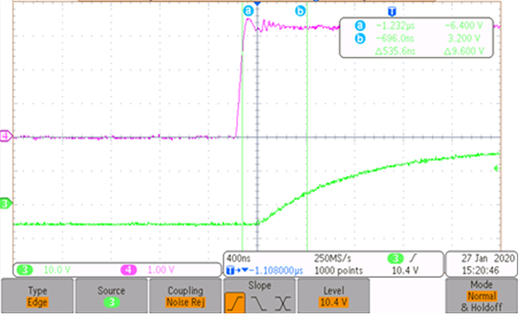 Figure 5-5 Board 2 Propagation Delay VIH to VTH
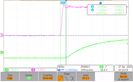 Figure 5-6 Board 2 Propagation Delay Start to Start
Both the boards have around 540-ns propagation delay from VIH to VTH. However, measured from the start of waveforms, Board 1 has a lower delay of 100 ns compared to 180 ns for Board 2.
The thermal performance of the boards with no airflow while driving 1 µF at 10 kHz is shown in Figure 5-7 and Figure 5-8.
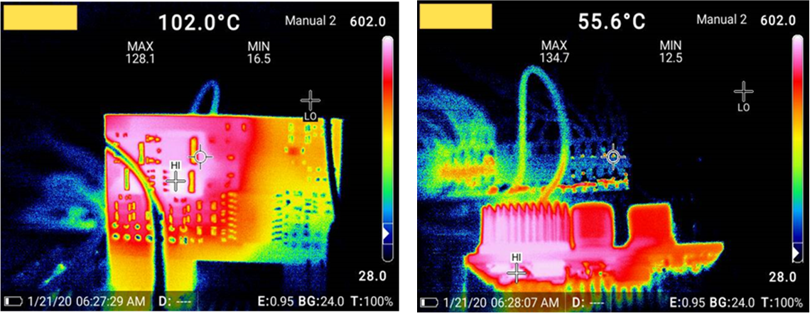 Figure 5-7 Board 1 Thermal Profile
Figure 5-7 shows that the driver transistors are the hottest components and that the temperature goes as high as 135°C.
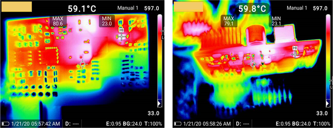 Figure 5-8 Board 2 Thermal Profile
Figure 5-8 shows that the flyback converter IC is the hottest component with a temperature of around 80°C.
Board 2 bootstrap (C27) voltage variation while driving 1 µF. Red – PWM input, Blue – C27 voltage, Green – output voltage across the 1-µF capacitor.
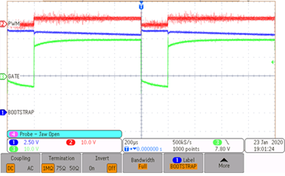 Figure 5-9 Bootstrap Voltage at 1 kHz
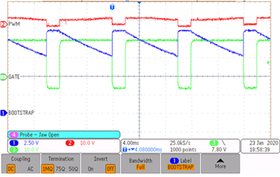 Figure 5-10 Bootstrap Voltage at 100 Hz
There is very little droop in voltage at 1 kHz. Even at 100 Hz, the minimum voltage is maintained above 7.5 V at 80% duty cycle and hence no noticeable effect in the output waveform.
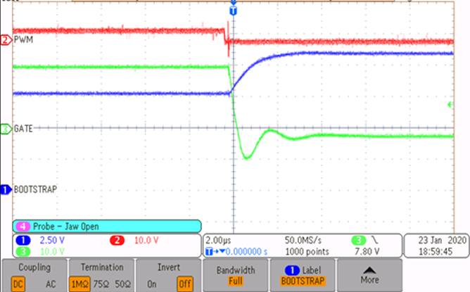 Figure 5-11 Bootstrap Voltage Charging Time
The bootstrap capacitor gets charged in around 1 µs.
Board 1 Miller clamping: Driving 470 nF with 18 Ω. Magenta – clamp current, Green – drive voltage.
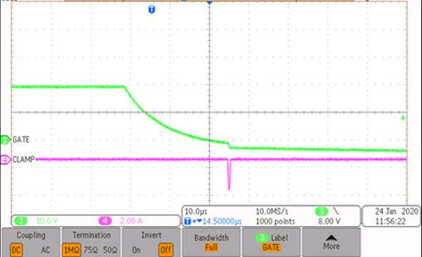 Figure 5-12 Miller Clamp Current
The Miller clamp is able to hold the gate voltage close to the negative bus in spite of the high gate-drive impedance. Gate-drive resistance is intentionally made around 18 Ω to push some current into the clamp. For effectiveness of the Miller clamp, the transistor must be placed as close as possible to the gate and source terminals.
Board 1 DESAT slow turn-off operation while driving 470 nF with 1-Ω drive resistance. Blue – PWM input, Green – Output voltage, Magenta – DESAT input.
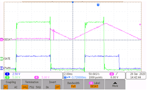 Figure 5-13 DESAT Turn off Without R16 and C20
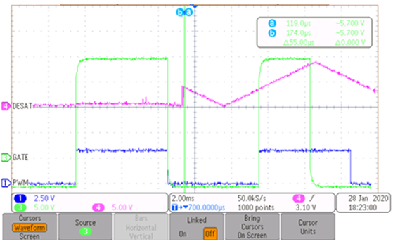 Figure 5-14 DESAT Turn off With R16 and C20
The R-C network at the OUTL pin helps restore slow turn-off operation with external current boosting.