SLUA560D June 2011 – March 2022 UCC28950 , UCC28950-Q1 , UCC28951 , UCC28951-Q1
- Trademarks
- 1 Design Specifications
- 2 Functional Schematic
- 3 Power Budget
- 4 Transformer Calculations (T1)
- 5 QA, QB, QC, QD FET Selection
- 6 Selecting LS
- 7 Output Inductor Selection (LOUT)
- 8 Output Capacitance (COUT)
- 9 Select FETs QE and QF
- 10Input Capacitance (CIN)
- 11Setting Up the Current Sense (CS) Network (CT, RS, RRE, DA)
- 12Voltage Loop and Slope Compensation
- 13Setting Turn-on Delays to Achieve Zero Voltage Switching (ZVS)
- 14Turning SR FETs-off Under Light Load Conditions
- 15600 W FSFB Detailed Schematic and Test Data
- 16References
- 17Revision History
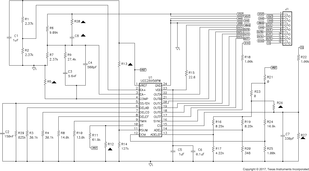
15 600 W FSFB Detailed Schematic and Test Data
 Figure 15-1 Daughter
Board Schematic
Figure 15-1 Daughter
Board SchematicBlack triangles designate not populated.
It is recommended to use an RCD clamp to protect the output synchronous FETs from over voltage due to switch node ringing. This RCD clamp is formed by diodes D4, D6 and resistor R6, R8 and R9 and capacitor C1.
Full bridge gate drives and primary switch nodes (QBd and QDd) at VIN = 390 V, IOUT = 5 A.
Full bridge gate drives and switch nodes at VIN = 390 V, IOUT = 10 A
Switch node QBd/Q4d is valley switching and node QDd/Q3d has achieved ZVS. It is not uncommon for switch node QDd/Q3d to obtain ZVS before QBd/Q4d. This is because during the QDd/Q3d switch node voltage transition, the reflected output current provides immediate energy for the LC tanking at the switch node. Where at the QBd/Q4d switch node transition the primary has been shorted out by the high side or low side FETs in the H bridge. This transition is dependent on the energy stored in LS and LLK to provide energy for the LC tanking at switch node QBd/Q4d making it take longer to achieve ZVS.
Full bridge gate drives and switch nodes at VIN = 390 V, IOUT = 25 A
When the converter is running at 25 A both switch nodes are operating into zero voltage switching (ZVS). It is also worth mentioning that there is no evidence of the gate miller plateau during gate driver switching. This makes sense because the voltage across the drain and source of FETs QA through QD has already transition before the gate drives have transitioned.
Full bridge gate drives and switch nodes at VIN = 390 V, IOUT = 50 A
ZVS was maintained from 50% to 100% output power.