SLUA560D June 2011 – March 2022 UCC28950 , UCC28950-Q1 , UCC28951 , UCC28951-Q1
- Trademarks
- 1 Design Specifications
- 2 Functional Schematic
- 3 Power Budget
- 4 Transformer Calculations (T1)
- 5 QA, QB, QC, QD FET Selection
- 6 Selecting LS
- 7 Output Inductor Selection (LOUT)
- 8 Output Capacitance (COUT)
- 9 Select FETs QE and QF
- 10Input Capacitance (CIN)
- 11Setting Up the Current Sense (CS) Network (CT, RS, RRE, DA)
- 12Voltage Loop and Slope Compensation
- 13Setting Turn-on Delays to Achieve Zero Voltage Switching (ZVS)
- 14Turning SR FETs-off Under Light Load Conditions
- 15600 W FSFB Detailed Schematic and Test Data
- 16References
- 17Revision History
12 Voltage Loop and Slope Compensation
The UCC28950/1 VREF output (Pin 1) needs a high frequency bypass capacitor to filter out high frequency noise. This pin needs at least 1 µF of high frequency bypass capacitance (CBP1). Please refer to figure 1 for proper placement.
The voltage amplifier reference voltage (Pin 2, EA +) can be set with a voltage divider (RA, RB), for this design example we are going to set the error amplifier reference voltage (V1) to 2.5 V. Select a standard resistor value for RB and then calculate resistor value RA.
UCC28950/1/1 reference voltage:
Set voltage amplifier reference voltage:
Voltage divider formed by resistor RC and RI are chosen to set the DC output voltage (VOUT) at Pin 3 (EA-).
Select a standard resistor for RC:
Calculate RI:
Then choose a standard resistor for RI:
Compensating the feedback loop can be accomplished by properly selecting the feedback components (RF, CZ and CP). These components are placed as close to pin 3 and 4 as possible of the UCC28950/1.
Calculate load impedance at 10% load (RLOAD):
Approximation of control to output transfer function (GCO(f)) as a function of frequency:
Double pole frequency of GCO(f):
Angular velocity:
Compensate the voltage loop with type 2 feedback network. The following transfer function is the compensation gain as a function of frequency (GC(f)). Please refer to Figure 2-1 for component placement.
Calculate voltage loop feedback resistor (RF) based on crossing the voltage (fC) loop over at a 10th of the double pole frequency (fPP).
Select a standard resistor for RF.
Calculate the feedback capacitor (CZ) to give added phase at crossover.
Select a standard capacitance value for the design.
Put a pole at two times fC.
Select a standard capacitance value for the design.
Loop gain as a function of frequency (TV(f)) in dB.
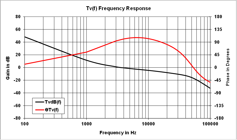
Plot theoretical loop gain and phase to graphically check for loop stability (Figure 11-1). The theoretical loop gain crossed over at roughly 3.7 kHz with a phase margin of greater than 90 degrees.
It is wise to check your loop stability of your final design with transient testing and/or a network analyzer and adjust the compensation (GC(f)) feedback as necessary.
 Figure 12-1 Loop Gain
and Loop Phase
Figure 12-1 Loop Gain
and Loop PhaseTo limit over shoot during power up the UCC28950/1 has a soft-start function (SS, Pin 5) which in this application was set for a soft start time of 15 ms (tSS).
Select a standard capacitor for the design.
The UCC28950/1 also provides slope compensation for peak current mode control (Pin 12). This can be set by setting RSUM with the following equations. The following equations will calculate the required amount of slope compensation (VSLOPE) that is needed for loop stability.
The change in magnetizing current on the primary ΔILMAG contributes to slope compensation.
To help improve noise immunity VSLOPE is set to have a total slope that will equal 10% of the maximum current sense signal (0.2 V) over one inductor switching period.
If VSLOPE2 < VSLOPE1 set VSLOPE = VSLOPE1
If VSLOPE2 ≥ VSLOPE1 set VSLOPE = VSLOPE2
Select a standard resistor for RSUM.