SLUS720F February 2007 – June 2019 TPS40195
PRODUCTION DATA.
- 1 Features
- 2 Applications
- 3 Description
- 4 Revision History
- 5 Description (continued)
- 6 Pin Configuration and Functions
- 7 Specifications
- 8 Detailed Description
-
9 Application and Implementation
- 9.1 Application Information
- 9.2
Typical Applications
- 9.2.1
Typical Application 1
- 9.2.1.1 Design Requirements
- 9.2.1.2
Detailed Design Procedure
- 9.2.1.2.1 Output Inductor, LOUT
- 9.2.1.2.2 Output Capacitor, COUT
- 9.2.1.2.3 Input Capacitor, CIN
- 9.2.1.2.4 Switching MOSFET, QSW
- 9.2.1.2.5 Rectifier MOSFET, QSR
- 9.2.1.2.6
Component Selection for the TPS40195
- 9.2.1.2.6.1 Timing Resistor, RT
- 9.2.1.2.6.2 Setting UVLO
- 9.2.1.2.6.3 Setting the Soft-Start Time
- 9.2.1.2.6.4 Short-Circuit Protection, RILIM
- 9.2.1.2.6.5 Voltage Decoupling Capacitors, CBP, and CVDD
- 9.2.1.2.6.6 Boost Voltage, CBOOST and DBOOST (optional)
- 9.2.1.2.6.7 Closing the Feedback Loop RZ1, RP1, RPZ2, RSET1, RSET2, CZ2, CP2 AND CPZ1
- 9.2.1.2.7 Application Curve
- 9.2.2 Typical Application 2
- 9.2.3 Typical Application 3
- 9.2.1
Typical Application 1
- 10Layout
- 11Device and Documentation Support
- 12Mechanical, Packaging, and Orderable Information
8.3.3 Oscillator and Synchronization
The TPS40195 has a programmable switching frequency of 100 kHz to 600 kHz using a resistor connected from the RT pin to GND. The relationship between switching frequency and the resistor from RT to GND is given in Equation 1.

where
- fSW is the switching frequency in kHz
- RRT is the resistor connected from RT to GND in kΩ
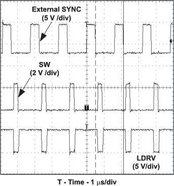
When the oscillator is programmed using this method, the SYNC pin is configured as an input. The device may be synchronized to a higher frequency than the free running frequency by applying a pulse train to the SYNC pin. For best results, limit the frequency of the pulse train applied to SYNC to 20% more than the free running frequency. The TPS40195 will synchronize to the falling edge of the pulse train applied to the SYNC pin.
The SYNC pin can also function as an output. To get this functionality, the RT pin must be connected to either GND or to BP. When this is done the oscillator will run at either 250 kHz or 500 kHz. SYNC can then be connected to other TPS40195 controllers (with their SYNC pins configured as an input) and the two or more controllers will synchronize to the same switching frequency. The output waveform on SYNC will be approximately a 50% duty cycle pulse train. The pull up is relatively weak, but the pull down is strong to insure that a good clean signal is presented to any devices that are to be synchronized. A summary is shown in Table 1.
Table 1. RT Connection and SYNC Pin Function
| RT CONNECTION | SYNC PIN FUNCTION | SWITCHING FREQUENCY |
|---|---|---|
| Resistor to GND | Input | See Equation 1 |
| GND | Output | 250 kHz |
| BP | Output | 500 kHz |
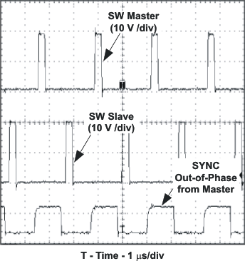
Using the TPS40195 with its RT pin connected to BP or to GND as a master clock source for another TPS40195 with a resistor connected from its RT pin to GND results in the two controllers operating at the same frequency but 180° out of phase.
 Figure 18. TPS40195 Synchronized to External SYNC Pin Pulse (Negative Edge Triggered)
  Figure 19. TPS40195 SYNC Pin Master/Slave Configuration. 180° Out-of-Phase Operation