SLUS720F February 2007 – June 2019 TPS40195
PRODUCTION DATA.
- 1 Features
- 2 Applications
- 3 Description
- 4 Revision History
- 5 Description (continued)
- 6 Pin Configuration and Functions
- 7 Specifications
- 8 Detailed Description
-
9 Application and Implementation
- 9.1 Application Information
- 9.2
Typical Applications
- 9.2.1
Typical Application 1
- 9.2.1.1 Design Requirements
- 9.2.1.2
Detailed Design Procedure
- 9.2.1.2.1 Output Inductor, LOUT
- 9.2.1.2.2 Output Capacitor, COUT
- 9.2.1.2.3 Input Capacitor, CIN
- 9.2.1.2.4 Switching MOSFET, QSW
- 9.2.1.2.5 Rectifier MOSFET, QSR
- 9.2.1.2.6
Component Selection for the TPS40195
- 9.2.1.2.6.1 Timing Resistor, RT
- 9.2.1.2.6.2 Setting UVLO
- 9.2.1.2.6.3 Setting the Soft-Start Time
- 9.2.1.2.6.4 Short-Circuit Protection, RILIM
- 9.2.1.2.6.5 Voltage Decoupling Capacitors, CBP, and CVDD
- 9.2.1.2.6.6 Boost Voltage, CBOOST and DBOOST (optional)
- 9.2.1.2.6.7 Closing the Feedback Loop RZ1, RP1, RPZ2, RSET1, RSET2, CZ2, CP2 AND CPZ1
- 9.2.1.2.7 Application Curve
- 9.2.2 Typical Application 2
- 9.2.3 Typical Application 3
- 9.2.1
Typical Application 1
- 10Layout
- 11Device and Documentation Support
- 12Mechanical, Packaging, and Orderable Information
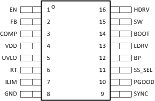
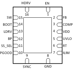
6 Pin Configuration and Functions
PW Package
16-Pin TSSOP
Top View

RGY Package
16-Pin VQFN
Top View

Pin Functions
| PIN | I/O | DESCRIPTION | |
|---|---|---|---|
| NAME | NO. | ||
| BOOT | 14 | I | Gate drive voltage for the high-side N-channel MOSFET. A 100-nF capacitor (typical) must be connected between this pin and SW. |
| BP | 12 | O | Output bypass for the internal regulator. Connect a capacitor of 1-μF (or greater) from this pin to GND. Larger capacitors, up to 4.7μF will improve noise performance with a low side FET Qg over 25nC. Do not connect to VDD or drive externally. This regulator is turned off when ENABLE is pulled low |
| COMP | 3 | O | Output of the error amplifier. |
| EN | 1 | I | Logic level input which starts or stops the controller from an external user command. A high-level turns the controller on. A weak internal pull-up holds this pin high so that the pin may be left floating if this function is not used. Observe interface cautions in applications information. |
| FB | 2 | I | Inverting input to the error amplifier. In normal operation the voltage on this pin is equal to the internal reference voltage (591 mV typical) |
| GND | 8 | - | Common reference for the device |
| HDRV | 16 | O | Gate drive output to the high-side N-channel FET. |
| ILIM | 7 | I | Current limit. Sets short circuit protection threshold for low-side MOSFET sensing. Connect a resistor to GND to set the threshold |
| LDRV | 13 | O | Gate drive output for the low side N-channel FET. |
| PGOOD | 10 | O | Open drain power good output. Pulls low under any fault condition, soft start is active or if the FB pin voltage is outside the specified voltage window. |
| RT | 6 | I | Switching frequency programming pin. Also determines function of SYNC pin. Connected to GND for 250 kHz operation and using SYNC as an output. Connect to BP for 500-kHz operation and using SYNC as an output. Connect a resistor to GND to program a frequency and allow SYNC to accept synchronization pulses. If RT is used to program a switching frequency and SYNC is not to be used to synchronize the converter to an external clock, connect SYNC to GND. |
| SS_SEL | 11 | I | Soft-start timing selection. Can be connected to GND, BP or left floating to select a soft start time that is proportional to the switching frequency. |
| SW | 15 | I | Sense line for the adaptive anti-cross conduction circuitry. Serves as common connection for the flying high-side MOSFET driver |
| SYNC | 9 | I/O | Bidirectional synchronization I/O pin. SYNC is an output when the RT pin is connected to BP or GND. The output is a falling edge signal 180° out-of-phase with the rising edge of HDRV. In this mode SYNC can be used to drive the SYNC pin of an additional TPS40195 device whose RT pin is tied to GND through a resistor, providing two converters that operate 180° out-of-phase to one another. SYNC may be used as an input to synchronize to an external system clock if RT is connected to GND through a resistor as well. The device synchronizes to the falling edge of the external clock signal. If RT is used to program a switching frequency and SYNC is not to be used to synchronize the converter to an external clock, connect SYNC to GND. |
| UVLO | 5 | I | Programmable UVLO pin for the controller. A resistor divider on this pin to VDD sets the converter turn on voltage and the hysteresis for turnoff. |
| VDD | 4 | I | Power input to the controller. A 100-nF bypass capacitor should be connected closely from this pin to GND. |