SLVT248 May   2026  – May 2026


  1.   1
  2.   Description
  3.   Resources
  4.   Features
  5.   Applications
  6. 1Test Prerequisites
    1. 1.1 Voltage and Current Requirements
    2. 1.2 Functional Block Diagram
    3. 1.3 Pin Functions
    4. 1.4 Required Equipment
    5. 1.5 Dimensions
    6. 1.6 Test Setup
  7. 2Testing and Results
    1. 2.1 Efficiency Graphs
    2. 2.2 Efficiency Data
    3. 2.3 Voltage Regulation
    4. 2.4 Thermal Images
  8. 3Waveforms
    1. 3.1 Switching
    2. 3.2 Output Voltage Ripple
    3. 3.3 Short-Circuit Protection
    4. 3.4 Load Transients
    5. 3.5 Start-Up and Shutdown Sequence
    6. 3.6 Brown In and Brown Out
  9.   Trademarks

Switching

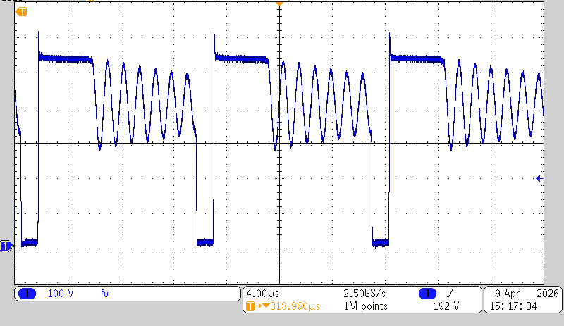
Switching behavior is shown in Figure 3-1 through Figure 3-7.


PMP41184 127 VDC, 100% LOAD, Vsw

Figure 3-1 127 VDC, 100% LOAD, Vsw
PMP41184 400 VDC, 75% LOADFigure 3-3 400 VDC, 75% LOAD
PMP41184 400 VDC, 25% LOAD, VswFigure 3-5 400 VDC, 25% LOAD, Vsw
PMP41184 400 VDC, No LOAD, VswFigure 3-7 400 VDC, No LOAD, Vsw
PMP41184 400 VDC, 100% LOAD, VswFigure 3-2 400 VDC, 100% LOAD, Vsw
PMP41184 400 VDC, 50% LOAD, VswFigure 3-4 400 VDC, 50% LOAD, Vsw
PMP41184 400 VDC, 10% LOAD, VswFigure 3-6 400 VDC, 10% LOAD, Vsw