SLYY081B March 2018 – January 2024 AMC1305M25 , AMC1311 , AMC1311-Q1 , ISO1042 , ISO1042-Q1 , ISO5851 , ISO7741 , ISO7841 , ISOM8710 , UCC20225-Q1 , UCC20225A-Q1 , UCC21520 , UCC21540 , UCC23513 , UCC5390
Failure mode 2: Test results
To verify that TI reinforced isolation technology exhibits a “fail open” behavior for stress conditions where the safety-limiting current or power parameters are violated, several tests were performed. For experiments 1 and 2, ISO5851, a reinforced isolated gate-driver, and ISO7841, a reinforced quad-channel digital isolator were chosen.
In experiment 1, the isolator’s output pins were short circuited, while raising the isolator’s supply voltage until the isolator was no longer functional.
In experiment 2, using a surge generator, a repetitive high-voltage strikes (1 kV and 2 kV) was applied to one-side of the isolator. This was to simulate the impact of short circuits to high-voltage DC buses in motor drive, solar inverter, and other similar applications.
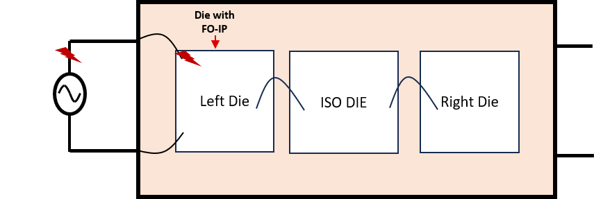
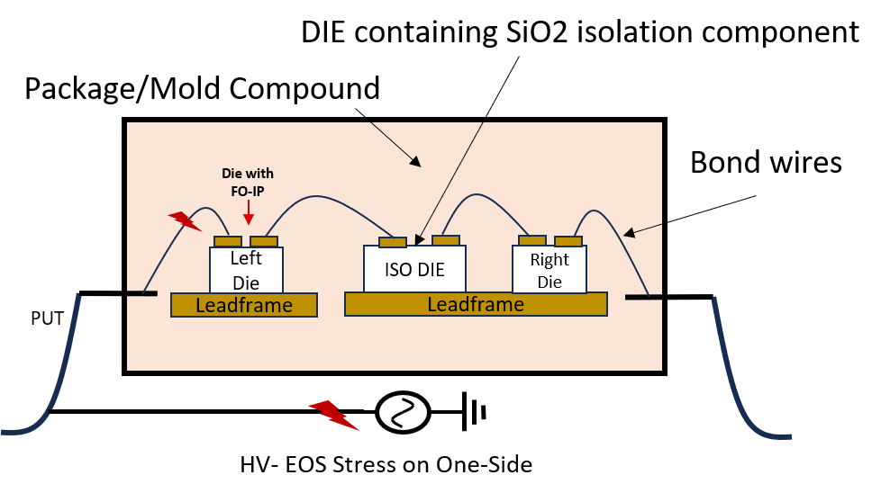
TI has also implemented a new “fail open” feature on the input die for products such as the ISOM8710 Opto-emulator where the isolation is based on a 3-die solution as shown in Figure 8. This new feature ensures that the insulation barrier and output-die are protected under input-side EOS events. Figure 9 provides a cross-sectional view of the 3-die opto-emulator with the input fail open IP.
 Figure 8 High voltage stress applied on one side of the 3-die isolator. The left die designed with fail-open (FO) IP ensures integrity of ISO die and the right die under EOS events.
 Figure 9 Cross-sectional view of the 3-die opto-emulator with Fail-Open IP.
 To demonstrate the fail open feature, input die with three EOS types was stressed in experiments 3-5 and looked at isolation integrity post stress.
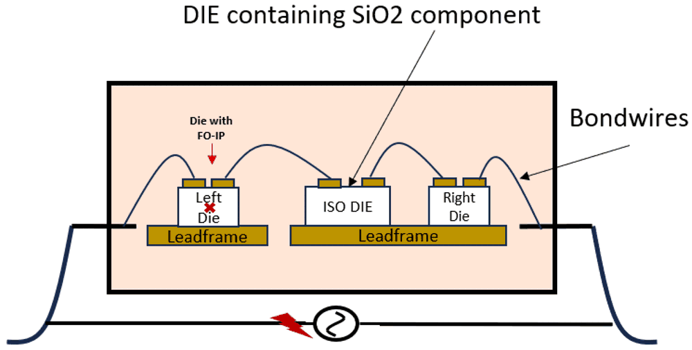
In experiment 3, EOS voltage was applied to the input-side (between Anode and Cathode) at room and high temperature using a DC supply through different source impedances for 10 minutes, which causes the input-die to fail-open. This emulates a DC-EOS event that can persist until system shutdown. Next, EOS was applied for 12 hours to ensure input-die remains fail-open even for prolonged EOS stress on the open device. Finally, ramp to breakdown test (RTB) was conducted on the insulation barrier to check isolation integrity post functional failure caused by EOS event on the left die. Figure 10 shows the RTB setup where we apply HV stress across isolation barrier.
 Figure 10 HV Ramp-to-Breakdown (RTB) across Isolation.
In experiment 4, the EOS-input is changed from experiment 3 with similar test procedure. We connected pre-charged capacitors to study the impact of capacitor discharge on the input side of the isolation.
In experiment 5, a current source was applied to the input side and ramped it up until fail open on the input side. Experiments 3 to 5 simulate DC-supply bus shorts to the input side in the above applications.
Fail-open feature is also implemented on the output-die pins (VDD, OUT1, and OUT2) in ISO-comparators such as AMC23C10 where the isolation is based on single die reinforced isolation capacitor approach as shown in Figure 6. Experiments 3-5 were also performed on these parts to ensure input die and isolation are both intact post functional failure of output die from EOS events. The results are summarized in Table 1.
Table 1 lists the results of these experiments. In all cases, after the high-power stress, all isolators maintained a high-impedance between side 1 and side 2. That is, they “fail open.” Additionally, ISO5851 and ISO7841 were further tested for basic isolation rating of 3 kVRMS for 60 seconds. All devices were able to withstand this voltage without breakdown. ISOM8710 were further tested in ramp-to-breakdown in oil post stress. In other words, basic isolation was preserved after the high-power test. As an extreme test, 50 2-kV surge impulses of both positive and negative polarity were applied to two units each of the gate driver and digital isolator. Even after such a severe stress, the isolators maintained high impedance between side 1 and side 2, maintained basic isolation, and “failed open.”
| Experiment number | Device | Test description | Number of devices | Observation | Post-stress RIO | Post-stress VISO 60-s test, 3 kVRMS |
|---|---|---|---|---|---|---|
| 1,2 | ISO5851 | Gate-driver output shorted to side-2 ground. Supply was raised to 50 V until device became damaged | 5 | Die 3 damaged | >1TΩ | Passed |
| 2kV surge on gate-driver output, 5 times each polarity (+ve and - ve) | 5 | Die 3 damaged | >1TΩ | Passed | ||
| 2kV surge on gate-driver output, 50 times each polarity (+ve and - ve) | 2 | Die 3 damaged | >1TΩ | Passed | ||
| 1,2 | ISO7841 | All side-2 pins shorted to side-2 ground or supply, or were left floating. Supply was raised to 25 V until the device became damaged. | 5 | Die 2 damaged | >1TΩ | Passed |
| 1kV or 2kV surge on all side-2 pins, 5 times each polarity (+ve and - ve) | 4 | Die 2 damaged | >1TΩ | Passed | ||
| 2kV surge on all side-1 pins, 5 times each polarity (+ve and - ve) | 2 | Die 1 damaged | >1TΩ | Passed | ||
| 2kV surge on all side-1 pins, 50 times each polarity (+ve and - ve) | 2 | Die 1 damaged | >1TΩ | Passed | ||
| 2kV surge on all side-1 pins, 500 times each polarity (+ve and - ve) | 1 | Die 2 damaged | >1TΩ | Passed | ||
| 3,4,5 | ISOM8710 | EOS applied to input side between pin-1 to ground with output side open. Different values of supply voltages up to 43 V and currents were tested until fail open on the input die. EOS was applied for 12 hours post fail and input die resistances were measured. Isolation integrity post stress was tested using RTB. | 270 | No isolation degradation, non-functional | >1TΩ | Passed |
| Connect a pre-charged 2.2 mF cap (30 V, 3A) between pin1 to ground. If fail-short continue driving up to 3A until input die fail open. Isolation integrity post stress was tested using RTB. | 5 | No isolation degradation, non-functional | >1TΩ | Passed | ||
| Apply graudally increasing current up to 3A to primary until input die fail open. In fail-short, continue feeding short until open. Isolation integrity post stress was tested using RTB. | 5 | No isolation degradation, non-functional | >1TΩ | Passed | ||
| 3,4,5 | AMC23C10 | EOS applied to input side between pin-1 to ground with output side open. Different values of supply voltages up to 36 V and currents were tested until fail open on the input die. EOS was applied for 24 hours post fail and input die resistances were measured. Isolation integrity post stress was tested using RTB. | 20 per pin 60 in total | No isolation degradation, non-functional | >1TΩ | Passed |
| Connect a pre-charged 2.2 mF cap (30 V, 3A) between pin1 to ground. If fail-short continue driving up to 3A until input die fail open. Isolation integrity post stress was tested using RTB. | 5 | No isolation degradation, non-functional | >1TΩ | Passed | ||
| Apply graudally increasing current up to 3A to primary until input die fail open. In fail-short, continue feeding short until open. Isolation integrity post stress was tested using RTB. | 5 | No isolation degradation, non-functional | >1TΩ | Passed |
After the high-power stress was applied, some of these devices were de-capsulated and photographed to check the internal state of each (see Figure 11 and Figure 12). The results are consistent with expectations from our failure analysis. While the die facing the high-power stress was substantially damaged, at least one-die with one isolation capacitor was completely preserved. This die was responsible for the “fail open” nature observed. In the case of ISO5851, being a three-die module, the damage was limited to the gate-driver die, and damage to the isolation barrier was minimal.