SLYY200A April 2021 – December 2023 LM25149 , LM25149-Q1 , LM5156-Q1 , LM5157-Q1 , LM53635-Q1 , LM60440-Q1 , LM61460-Q1 , LM61495-Q1 , LMQ62440-Q1 , LMR33630-Q1 , LMS3655-Q1 , TPS55165-Q1 , UCC12040 , UCC12050
- 1
- Overview
- At a glance
- What is EMI?
- Conventional methods to reduce EMI in the low- and high-frequency ranges
- Innovations in reducing low-frequency emissions
- Spread spectrum
- Active EMI filtering
- Cancellation windings
- Innovations in reducing high-frequency emissions
- HotRod™ package
- Enhanced HotRod QFN
- Integrated input bypass capacitor
- True slew-rate control
- EMI modeling capabilities
- Low-frequency EMI designs using WEBENCH® design tool
- Conducted and radiated EMI results published in data sheets
- Conclusion
- Keep product categories for low EMI
Cancellation windings
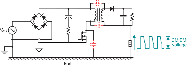
Unlike non-isolated converters, an additional emissions path across the isolation boundary is a key cause of common-mode (CM) EMI in isolated converters. Figure 15 on the following page shows the presence of the parasitic capacitances across the isolation transformer in a standard flyback converter. CM currents can flow directly from primary to earth through the parasitic capacitance associated with each switched node. The CM currents also flow from primary to secondary because of parasitic capacitance between the windings, causing an increase in the measured CM EMI. Conventionally, you could attenuate this additional disturbance by using a large CM choke in the input power path.
 Figure 15 CM EMI generating parasitics
in a flyback converter.
Figure 15 CM EMI generating parasitics
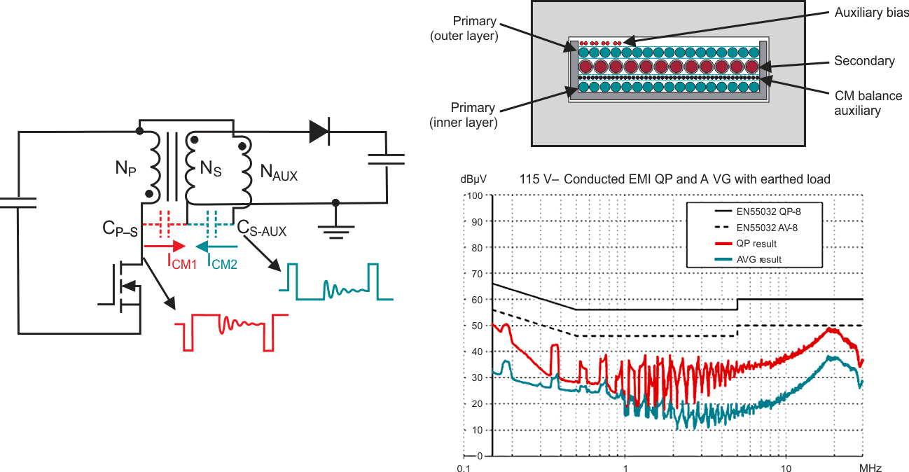
in a flyback converter.To help minimize the size of the passive filtering, the 65-W active clamp flyback with silicon FETs reference design for a high-power-density 5- to 20-V AC/DC adapter employs cancellation winding- and shielding-based approaches specific to isolated converters. As shown in Figure 16, an improved internal transformer structure has an extra auxiliary winding layer (shown in black) inserted in between the inner primary and secondary layers for CM balance. The auxiliary CM balance layer shields the inner half-primary to secondary interface and helps generate a canceling CM voltage to null the CM injection from the outer half-primary layer. Equalizing the parasitic capacitances to the secondary layer from the auxiliary winding and primary outer layers helps null the CM current injected into the secondary layer from the outer half-primary layer, by pushing an opposite-phase CM current from the cancellation layer. The net effect — close to zero CM current flowing into the secondary layer — reduces CM emissions, significantly helping the design meet EMI spectral standards with minimal CM filtering.
 Figure 16 Using shielding and
cancellation windings to reduce EMI in a flyback converter.