SLYY200A April 2021 – December 2023 LM25149 , LM25149-Q1 , LM5156-Q1 , LM5157-Q1 , LM53635-Q1 , LM60440-Q1 , LM61460-Q1 , LM61495-Q1 , LMQ62440-Q1 , LMR33630-Q1 , LMS3655-Q1 , TPS55165-Q1 , UCC12040 , UCC12050
- 1
- Overview
- At a glance
- What is EMI?
- Conventional methods to reduce EMI in the low- and high-frequency ranges
- Innovations in reducing low-frequency emissions
- Spread spectrum
- Active EMI filtering
- Cancellation windings
- Innovations in reducing high-frequency emissions
- HotRod™ package
- Enhanced HotRod QFN
- Integrated input bypass capacitor
- True slew-rate control
- EMI modeling capabilities
- Low-frequency EMI designs using WEBENCH® design tool
- Conducted and radiated EMI results published in data sheets
- Conclusion
- Keep product categories for low EMI
Conventional methods to reduce EMI in the low- and high-frequency ranges
Input voltage ripple generated by discontinuous currents in an SMPS can conduct to other systems when the systems share common physical contacts. Without proper mitigation, excessive input or output voltage ripple can compromise operation of the source, load or adjacent system. Traditionally, you could minimize the input ripple by using a passive inductor-capacitor (LC)-based EMI filter, as shown in Figure 4. An LC filter offers the required attenuation necessary to meet EMI specifications. The trade-off is a size and cost penalty for the system depending on the required attenuation, which will lower the overall power density. Also, large-sized inductors for input EMI filter design lose attenuation at frequencies greater than 30 MHz because of their lower self-resonant frequency, necessitating additional components like ferrite beads to handle the high-frequency attenuation.
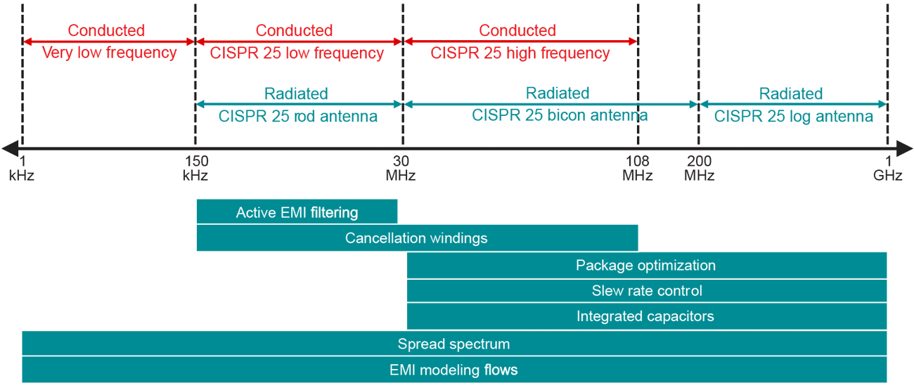
 Figure 3 A summary of the EMI mitigation techniques presented in this paper.
 Figure 4 A typical LC-based passive filter for EMI reduction, along with the
attenuation obtained.
Figure 4 A typical LC-based passive filter for EMI reduction, along with the
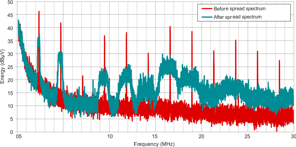
attenuation obtained.Another conventional approach to mitigating EMI is to use spread spectrum (or clock dithering) to modulate the switching frequency of an SMPS, which will reduce peaks in the frequency spectrum associated with the fundamental switching frequency and its harmonics — but at the expense of an increased noise floor, as shown in Figure 5.
 Figure 5 Example of the frequency spectrum of an SMPS with and without spread
spectrum.
Figure 5 Example of the frequency spectrum of an SMPS with and without spread
spectrum.Spread spectrum is an attractive technique, given its ease of implementation and the fact that you can use it in conjunction with other EMI reduction methods. It is not a panacea, however, as it can only provide relative reductions to existing EMI, and by nature its performance diminishes with lower switching frequencies. Furthermore, you can traditionally only apply spread spectrum to a single frequency band, for reasons that we will explore in the next section.
To minimize the size of the filter inductors, you can choose higher switching frequencies for your SMPS design. It is important to avoid sensitive frequency bands for switcher operation, however. For example, the preferred switching frequency for automotive power solutions has traditionally been in the sub-AM bands (approximately 400 kHz). Choosing a higher switching frequency to minimize inductor size means that you must avoid the entire AM band (525 to 1,705 kHz) so as to not have fundamental switching spurs in the more stringent automotive EMI frequency bands.
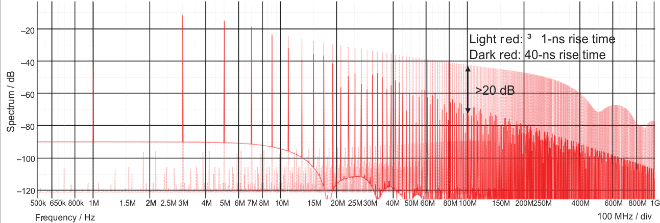
Switching converters from Texas Instruments (TI) have a switching frequency above 1.8 MHz to satisfy the EMI band requirements. The push to higher switching frequencies imposes a severe restriction on the switching transition rise and fall times to reduce switching losses. However, a switch node with very short rise and fall times maintains high energy content even at high frequencies close to its 100th harmonic, as shown in Figure 6, again highlighting the trade-off between high efficiency and low EMI.
 Figure 6 EMI plots of square waveforms with different rise times.
High slew rates will additionally result in high-frequency switch-node ringing, due to the presence of parasitic inductances in the power path of DC/DC converters, which further increases emissions at the ringing frequency and above. Figure 8 shows how the slew rate and the associated ringing on the switch node affect emissions. The traditional way to limit EMI emissions caused by the switching transition is to slow them down by adding intentional resistance in the gate-drive path of the switching device. This causes the transitions to happen more slowly, leading to faster roll-off of the emissions and an 8- to 10-dB reduction in emissions at the ringing frequency. This slowdown of the switching edges comes with a penalty of 2% to 3% in the peak current efficiency of the switching converter, however.