SNLA308A April 2019 – October 2020 DS90UB941AS-Q1 , DS90UH941AS-Q1
- Trademarks
- 1 Introduction
- 2 Superframe Requirements
- 3 Video Processing Status Monitoring
- 4 Superframe Splitting
-
5 Frame Cropping
- 5.1
Cropping Control Registers
- 5.1.1 CROP_START_X0_CROP_START_X0_P1 Register (Address = 36h) [reset = 0h]
- 5.1.2 CROP_START_X1_CROP_START_X1_P1 Register (Address = 37h) [reset = 0h]
- 5.1.3 CROP_STOP_X0_CROP_STOP_X0_P1 Register (Address = 38h) [reset = 0h]
- 5.1.4 CROP_STOP_X1_CROP_STOP_X1_P1 Register (Address = 39h) [reset = 0h]
- 5.1.5 CROP_START_Y0_CROP_START_Y0_P1 Register (Address = 3Ah) [reset = 0h]
- 5.1.6 CROP_START_Y1_CROP_START_Y1_P1 Register (Address = 3Bh) [reset = 0h]
- 5.1.7 CROP_STOP_Y0_CROP_STOP_Y0_P1 Register (Address = 3Ch) [reset = 0h]
- 5.1.8 CROP_STOP_Y1_CROP_STOP_Y1_P1 Register (Address = 3Dh) [reset = 0h]
- 5.2 Cropping Options
- 5.1
Cropping Control Registers
- 6 Splitter Mode Pixel Clocks
- 7 Programming Example
- 8 Summary
- 9 References
- 10Handling Interrupts With the DS90Ux941AS-Q1
-
11High-Speed GPIO Operation in Splitter Mode
- 11.1 Introduction
- 11.2 High-Speed Control Configuration
- 11.3 Back Channel Frequency Configuration
- 11.4 Splitter Mode GPIO
- 11.5 GPIO_0_Config Register (Address = Dh) [reset = 20h]
- 11.6 GPIO_1_and_GPIO_2_Config Register (Address = Eh) [reset = 0h]
- 11.7 GPIO_3_Config Register (Address = Fh) [reset = 0h]
- Revision History
10.2 Handling Interrupts in Splitter Mode Using Remote Interrupt Pin (REM_INTB)
The DS90Ux941AS-Q1 includes a dedicated remote interrupt pin (REM_INTB). This pin provides a pass-through of the INTB signal from an attached FPD-Link III deserializer (for example, the DS90Ux948-Q1). During a valid link connection, the value of the deseralizer INTB_IN is reflected to the DS90Ux941-Q1 REM_INTB pin. In Dual FPD3 mode, the REM_INTB pin indicates the INTB_IN from the attached dual-capable deserializer.
If multiple deserializers are connected, the REM_INTB typically indicates a combined interrupt from INTB_IN pins of multiple deserializers. The combined interrupt is asserted if either connection reports a remote interrupt. If desired, the Remote Interrupt Control (REM_INTB_CTRL, address 0x30) allows independent remote interrupts from both deserializers. Figure 10-2 shows a typical diagram for the receiver interrupt propagation for independent remote interruption.
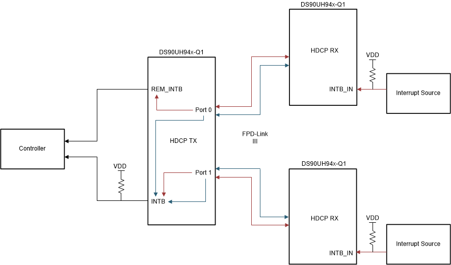 Figure 10-2 Interrupt Propagation in Splitter Mode Block Diagram
Selection 0001 of REM_INTB_MODE field brings a port 0 remote interrupt to the REM_INTB pin, and a port 1 remote interrupt to the INTB pin. For the INTB pin, the remote interrupt is combined with the HDCP interrupt register sources, but HDCP interrupts are only active if they are enabled through the HDCP_ICR register.
Note that in splitter mode, the latching behavior and logic states differ on port 0 and port 1
Port 0 (REM_INTB):
- REM_INTB outputs the opposite logic level of INTB_IN at the remote deserializer
- REM_INTB does not latch like non-splitter mode
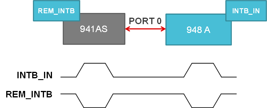 Figure 10-3 REM_INTB Logic in Splitter
Interrupt Mode
 Port 1 (INTB):
- INTB latches low after INTB_IN transitions from low to high
- INTB latch can be cleared to high by reading the HDCP_ISR register (0xC7)
- If INTB_IN is still high when 0xC7 is read, then the interrupt will not clear. INTB_IN must return to logic low before 0xC7 is read in order to clear the INTB latch
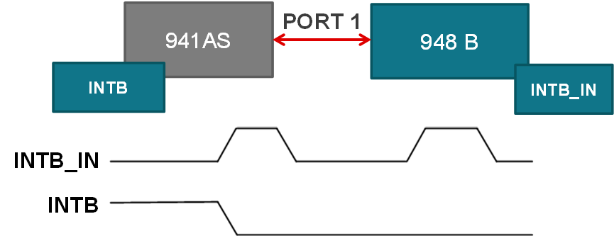 Figure 10-4 INTB Logic in Splitter
Interrupt Mode
Figure 10-4 INTB Logic in Splitter
Interrupt ModeThe sequence for handling the receiver interrupts in splitter mode is as follows:
Port 0:
- INTB_IN is pulled high or low by a downstream device on port 0
- The REM_INTB pin on the DS90Ux941AS-Q1 will output the opposite logic level of INTB_IN automatically
- Since REM_INTB does not latch in splitter mode, the system SW must be configured to ignore proceeding transitions until the interrupt is serviced
- The system SW can take action to access the remote interrupt source on port 0 (ex. Touch controller) to clear the INTB_IN signal back to the original low or high state
- REM_INTB will revert to the opposite logic level of INTB_IN
Port 1:
- INTB_IN is pulled high by a downstream device on port 1
- The INTB pin on the DS90Ux941AS-Q1 will transition from high to low and latch to the low state
- If the controller detects the INTB low and HDCP interrupt functionality is enabled, the controller reads the HDCP_ISR register to determine the interrupt source. This clears the interrupt at the HDCP Transmitter and releases the INTB, provided that the interrupt came from one of the HDCP Receiver devices.
- If INTB is still not cleared, then the interrupt came from a remote interrupt source attached to INTB_IN, and the controller must access the status register of the remote interrupt source (ex. Touch controller) to clear the downstream interrupt and return INTB_IN to logic low on port 1
- Once the INTB_IN pin returns to logic low on port 1, the controller reads he HDCP_ISR register to clear the INTB latch and return INTB to logic high on the DS90Ux941AS-Q1
If the above interrupt logic can not be used by the system, then alternatively standard GPIO mode may be used to signal interrupts from peripheral devices (ex. Touch controllers) attached to each remote deserializer in splitter mode. With standard GPIO signaling, neither signal will latch and the logic level of the remote GPIO signal will match the logic level of the local GPIO signal (no inversion). GPIO configuration is described in section 3.4
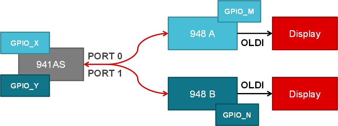 Figure 10-5 Example Splitter Mode
Interrupt Routing With Standard GPIO Signals.
 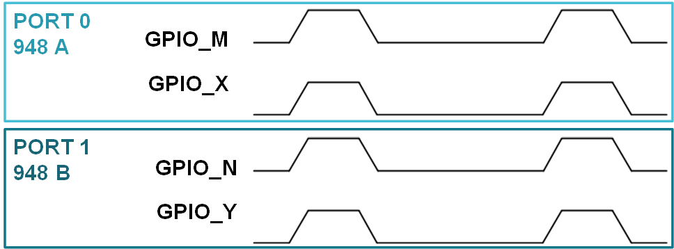 Figure 10-6 Example GPIO Logic with
Standard GPIO Pass-Throughs.