SNLA415 August 2022 DS160PT801
5.1 Receiver Detect (Rx Detect)
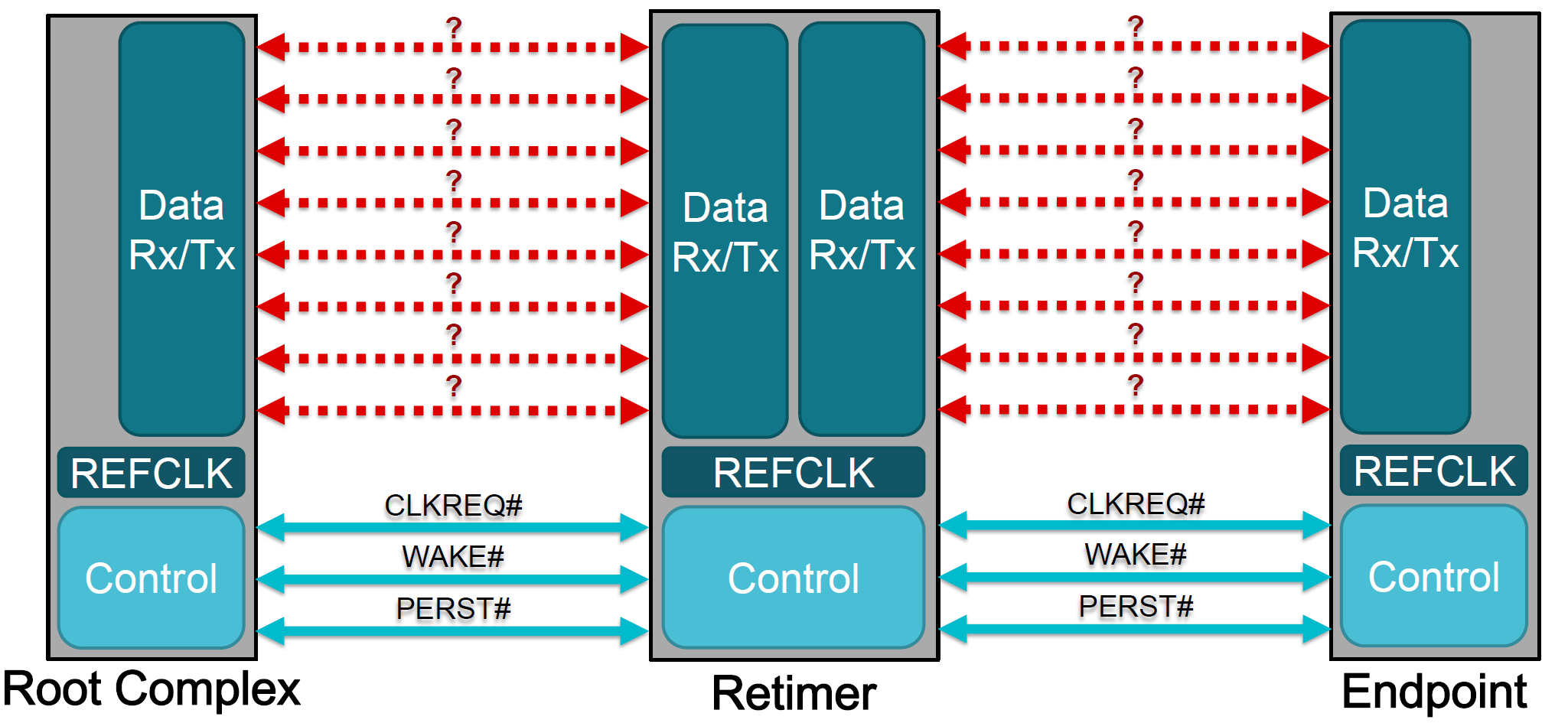
The first step in link training is receiver detection (Rx detect). Once all the devices are powered and have a reference clock provided, the devices start the Rx detect circuit on each lane that allows the device to determine if the device has a link partner to pair with. Figure 5-1 shows the diagram of PCIe devices trying to identify other PCIe devices to connect and send or receive data. Assuming that the PCIe Rx detect circuit sees the other device, each individual lane begins to transmit serial data at 2.5 Gbps. This is the lowest and most fundamental PCIe data rate, which was specified in the original PCIe Gen 1 specification. PCIe 1.0, also called PCIe Gen 1, is compatible with any PCIe device. So, every PCIe link begins with the same link initialization process. This also means that any PCIe device can transfer data at 2.5 Gbps if they can only form link at PCIe 1.0 data rate.
 Figure 5-1 PCIe Link Receiver
Detection