SNOAA61A October 2020 – February 2021 LMG3422R030 , LMG3422R050 , LMG3425R030 , LMG3425R050
3.1 Definition of RθJC/P for Package Thermal Performance
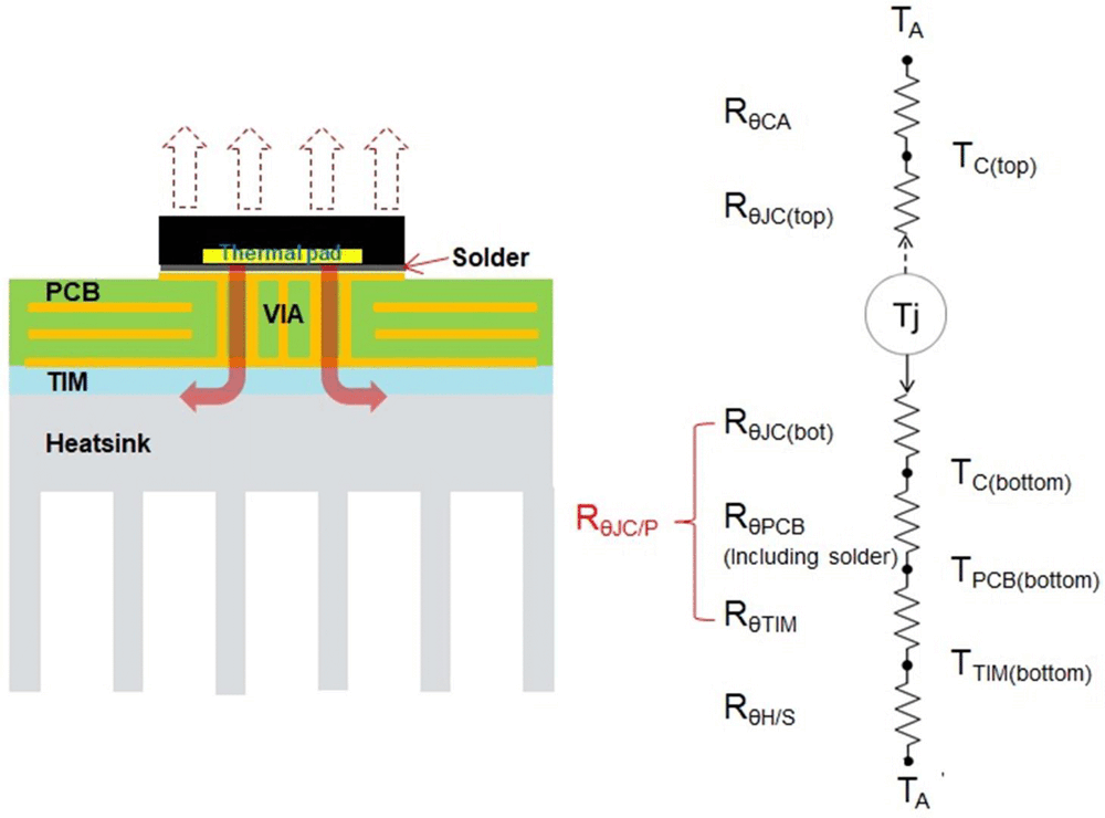
Two parallel heat flow paths from device
junction to ambient are depicted in Figure 3-1 with a corresponding
one-dimensional thermal resistance (Rθ) circuit model. Table 3-1 lists the descriptions for
various Rθ parameters indicated in Figure 3-1 and discussed in this
report. The bottom-side cooled QFN 12x12 package is designed to mainly dissipate heat from the
mounting PCB through thermal interface material (TIM) and attached heatsink to ambient.
Minimal heat is pulled away from package top to ambient in this typical bottom-side cooling
configuration. The more efficient the bottom path is, the less power is dissipated from the
top side.
Therefore, RθJA for an efficient
bottom-side cooled system can be estimated using Equation 1:
RθJC(bot or top), defined as the thermal resistance between device junction and package surface used for heat removal, is universally reported in manufacturers’ datasheet. However, using this parameter to compare package thermal performance directly is misleading under certain circumstances, especially among different types of packages. For example, the same 600-V Si MOSFET may have RθJC(bot) of 0.8 °C/W when packaged in D2PAK but of 0.6 °C/W in QFN 8x8, because D2PAK has a thicker Cu tab. This does NOT mean that thermally QFN 8x8 is a better package than D2PAK. Though increasing the package thermal resistance RθJC(bot), thicker Cu tab used in D2PAK package for die attachment can generate a more uniform heat distribution inside the package before heat flux reaches the PCB top Cu layer. Moreover, a larger thermal tab allows system designers to add more Cu pad area and thermal vias on PCB to reduce its thermal resistance. The RθTIM is lowered subsequently because of more effective heat spreading on PCB. Therefore, it is important that a well thermally-designed package could facilitate a better power dissipation capability at system level by improving the efficiency of existing cooling elements and/or enabling the use of more effective thermal solutions. For a bottom-side cooled, surface-mount package, its thermal performance is inevitably coupled to the mounting board (and attached TIM if used). To better define and compare thermal performance of different packages a practical indicator RθJC/P (i.e., thermal resistance from junction to major cooling plane) is used in the following sections, and is defined in Equation 2:
RθH/S or RθColdplate is excluded from Equation 2 for this definition because it is independent of device package design and more a function of its own characteristics (e.g., material and structure) and other use conditions such as flow rate of air/coolant.
 Figure 3-1 Typical Cooling Design for Surface-Mount
Device with Bottom Thermal Pad
Figure 3-1 Typical Cooling Design for Surface-Mount
Device with Bottom Thermal Pad| SYMBOL | DESCRIPTION |
|---|---|
| RθJA | Junction-to-ambient thermal resistance |
| RθJC(top) | Junction-to-case (top) thermal resistance |
| RθJC(bot) | Junction-to-case (bottom) thermal resistance |
| RθCA | Case-to-ambient thermal resistance |
| RθJC/P | Junction-to-cooling plane thermal resistance |
| RθPCB | Thermal resistance of PCB (including solder layer) |
| RθTIM | Thermal resistance of thermal interface material (TIM) |
| RθH/S | Thermal resistance of heatsink |