SNOAA61A October 2020 – February 2021 LMG3422R030 , LMG3422R050 , LMG3425R030 , LMG3425R050
2 New QFN 12x12 Package
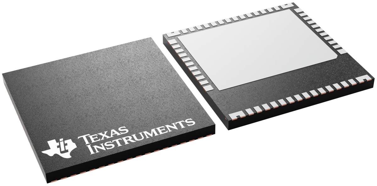
The newly developed QFN 12x12 is a low-profile, leadless surface-mount package with an exposed copper (Cu) thermal pad and functional pins on the package bottom surface shown in Figure 2-1. It maintains the same electrical merits and functional integrations as the prior QFN 8x8 package solution used for TI’s 600-V GaN power stage products. The improved package thermal design enables a high level of power dissipation and is implemented in this updated QFN 12x12 configuration.
 Figure 2-1 External Appearance of the QFN
12x12 Package (12 mm x 12 mm x 0.9 mm)
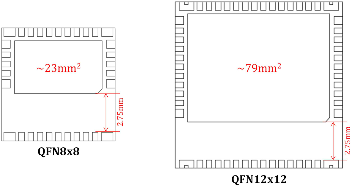
 Figure 2-2 Comparison of the Pin
Configuration on Package Bottom Surface
Figure 2-2 Comparison of the Pin
Configuration on Package Bottom SurfaceFigure 2-2 shows the QFN 12x12 package that has a 3x larger thermal pad area and the same creepage distance of 2.75 mm between the center thermal pad (tied to source internally) and bottom drain terminal pins compared to the preceding QFN 8x8 version. Table 2-1 compares the footprint and thermal pad area among TI’s QFN and other popular surface-mount packages; TO Lead-Less (TOLL) and D2PAK that are used for high-voltage GaN or silicon carbide (SiC) discrete devices. TI’s QFN 12x12 has the largest exposed thermal pad area of 79mm2 in comparison with competitors’ packages. Although occupying more real estate on the printed circuit board (PCB) than the TOLL package, it possesses a greater effective area that can be used for heat dissipation through a bottom-side cooling system by showing 7% more thermal pad area over PCB footprint ratio.
| MANUFACTURER | TI | TI | COMPETITOR A | COMPETITOR B |
|---|---|---|---|---|
| PACKAGE | QFN 8x8 | QFN 12x12 | TOLL 1 | D2PAK 2 |
| Minimum footprint on PCB (mm2) | 64 | 144 | 116 | 165 |
| Exposed thermal pad area (mm2) | 23 | 79 | 56 | 45 |
| Thermal pad area / PCB footprint (%) | 36 | 55 | 48 | 27 |
- 600V GaN HEMT
- 650V SiC MOSFET