SNOAAA8 April 2025 LM74610-Q1
4 Bench Test and Result
Figure 4-1 shows the LM74610-Q1 Bypass function application schematic with depletion MOSFET and Figure 4-2 shows the demo board top view with test modifications and setup.
 Figure 4-1 LM74610-Q1 Bypass Function Application
Schematic With Depletion MOSFET
 Figure 4-2 LM74610-Q1 Bypass Function Demo Board With
Depletion MOSFET
Figure 4-2 LM74610-Q1 Bypass Function Demo Board With
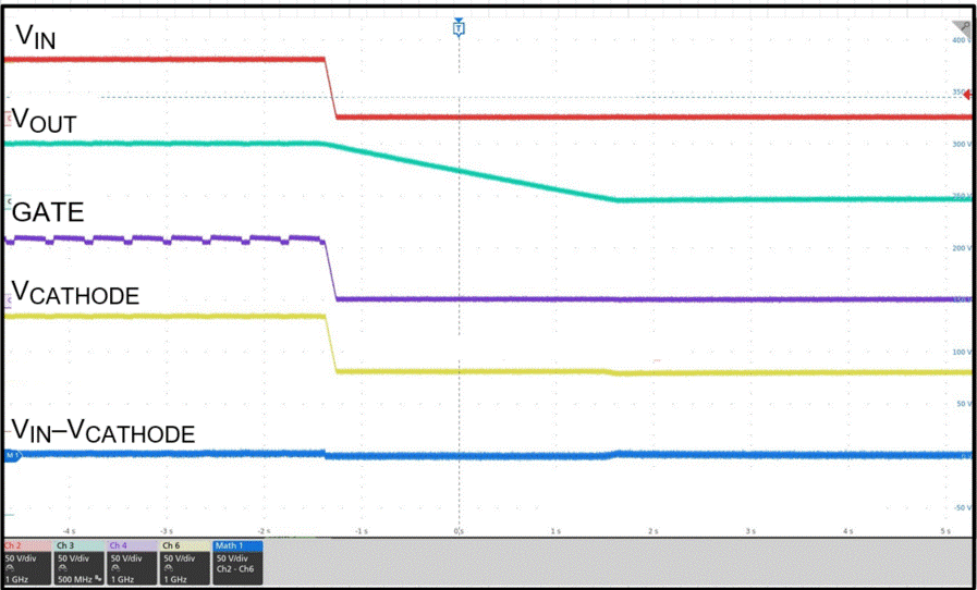
Depletion MOSFETFigure 4-3 shows test results for a 60V bypass switch design using the 40V LM74610-Q1 controller. With properly scaled MOSFETs (Q1 and QD), the input voltage range can extend to the VDS rating of the FETs. This enables high-voltage designs using the same low-voltage controller. Also, extending the input voltage range can also be useful in enterprise, communication, power tool and high-voltage battery-management applications.
 Figure 4-3 Test Result for a 60V Bypass
Circuit with LM74610 and Depletion MOSFET
Figure 4-3 Test Result for a 60V Bypass
Circuit with LM74610 and Depletion MOSFET| 60V bypass | LM74610-Q1 with depletion MOSFET | ||
| VIN ramped down from 60V to 0V | |||
| Device CATHODE pin follows (VIN + VT_QD) | |||
| Effective VANODE –VCATHODE clamped to VT of FET QD | |||