SNVSCP5C April   2025  – August 2026 TPS7H3024-SP , TPS7H3034-SP , TPS7H3124-SP , TPS7H3134-SP

PRODUCTION DATA  

  1.   1
  2. 1 Features
  3. 2 Applications
  4. 3 Description
  5. 4 Device Comparison Table
  6. 5 Pin Configuration and Functions
  7. 6 Specifications
    1. 6.1 Absolute Maximum Ratings
    2. 6.2 ESD Ratings
    3. 6.3 Recommended Operating Conditions
    4. 6.4 Thermal Information
    5. 6.5 Electrical Characteristics
    6. 6.6 Timing Requirements
    7. 6.7 Quality Conformance Inspection
    8. 6.8 Typical Characteristics
  8. 7 Parameter Measurement Information
  9. 8 Detailed Description
    1. 8.1 Overview
    2. 8.2 Functional Block Diagram
    3. 8.3 Feature Description
      1. 8.3.1 Input Voltage (IN), VLDO, and REFCAP
        1. 8.3.1.1 Undervoltage Lockout (VPOR_IN < VIN < UVLO)
        2. 8.3.1.2 Power-On Reset (VIN < VPOR_IN)
      2. 8.3.2 SR_UVLO
      3. 8.3.3 SENSEx Inputs
        1. 8.3.3.1 VTH_SENSEX and VOUTx_RISE
        2. 8.3.3.2 IHYS_SENSEx and VOUTx_FALL
        3. 8.3.3.3 Input to Output Time Diagrams
        4. 8.3.3.4 Top and Bottom Resistive Divider Design Equations
      4. 8.3.4 MODE
      5. 8.3.5 Output Stages (RESETx, PWRGD, WDO, PULL_UP1, and PULL_UP2)
        1. 8.3.5.1 Push-Pull Outputs
        2. 8.3.5.2 Open-Drain Outputs (TPS7H3124 and TPS7H3134)
      6. 8.3.6 WDI
      7. 8.3.7 User-Programmable TIMERS
        1. 8.3.7.1 DLY_TMR
        2. 8.3.7.2 WD_TMR
    4. 8.4 Device Functional Modes
  10. 9 Application and Implementation
    1. 9.1 Application Information
    2. 9.2 Typical Application
      1. 9.2.1 Window Voltage Monitoring
        1. 9.2.1.1 Design Requirements
        2. 9.2.1.2 Detailed Design Procedure
          1. 9.2.1.2.1 Input Power Supplies and Decoupling Capacitors
          2. 9.2.1.2.2 SR_UVLO Threshold
          3. 9.2.1.2.3 SENSEx Thresholds
        3. 9.2.1.3 Application Curves
      2. 9.2.2 Supervision of Negative Voltage Rails
        1. 9.2.2.1 Negative Voltage Monitoring Example
    3. 9.3 Power Supply Recommendations
    4. 9.4 Layout
      1. 9.4.1 Layout Guidelines
      2. 9.4.2 Layout Example
  11. 10Device and Documentation Support
    1. 10.1 Documentation Support
      1. 10.1.1 Related Documentation
    2. 10.2 Receiving Notification of Documentation Updates
    3. 10.3 Support Resources
    4. 10.4 Trademarks
    5. 10.5 Electrostatic Discharge Caution
    6. 10.6 Glossary
  12. 11Revision History
  13. 12Mechanical, Packaging, and Orderable Information

Output Stages (RESETx, PWRGD, WDO, PULL_UP1, and PULL_UP2)

The output stage's (RESET1 to RESET4), PWRGD and WDO are offered in push-pull and open-drain type. For more details on the output type by the GPN refer to Table 8-1. When the output are of overvoltage type, the RESETx is driven logically inverted from the output of the SENSEx comparators as shown in Figure 8-11 (also refer to Figure 8-16 and Figure 8-18).

In the case of the TPS7H3024 (push-pull outputs) and TPS7H3124 (open-drain outputs) with MODE=1, the SENSE1 (UV) and SENSE2 (OV) are internally AND'ed, the output is used to drive the RESET1 output. In this case RESET1 is the output of a window comparator. RESET2 is left unchanged and is the OV flag of SENSE2. As both the window and the OV flag are available, the system can read the outputs to known which type of fault occurred in the system (UV or OV). The same is true for SENSE3 and SENSE4, which form the second window comparator.
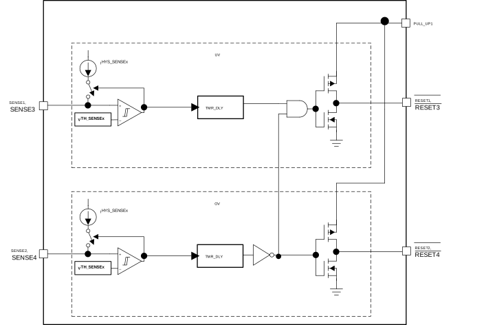
TPS7H3024-SP TPS7H3034-SP TPS7H3124-SP TPS7H3134-SP Window Comparator for TPS7H3024 when
          MODE=1 Figure 8-11 Window Comparator for TPS7H3024 when MODE=1
TPS7H3024-SP TPS7H3034-SP TPS7H3124-SP TPS7H3134-SP Window Comparator for TPS7H3124 when
          MODE=1 Figure 8-12 Window Comparator for TPS7H3124 when MODE=1
SENSE1 and SENSE2 are one window comparator channel while SENSE3 and SENSE4 create the second window comparator channel.