SNVU739A October 2020 – August 2021
6 Design Files
Figure 6-1 through Figure 6-6 illustrate the EVM PCB layout images.
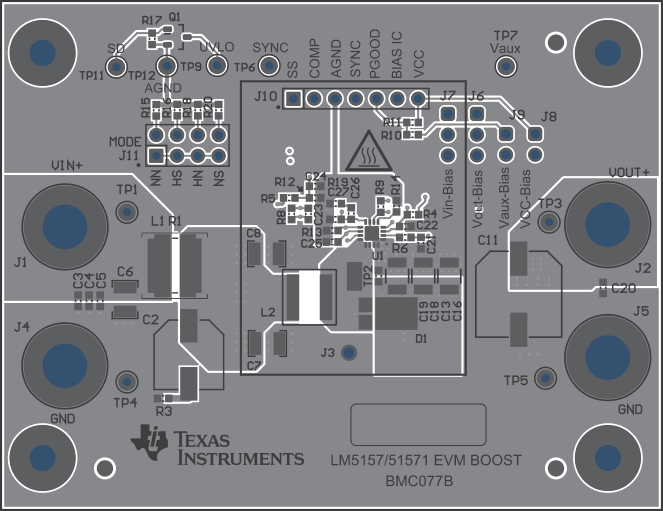 Figure 6-1 Top Layer and Silkscreen
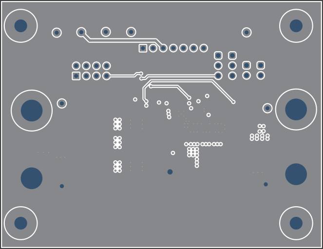 Figure 6-3 Signal Layer 1
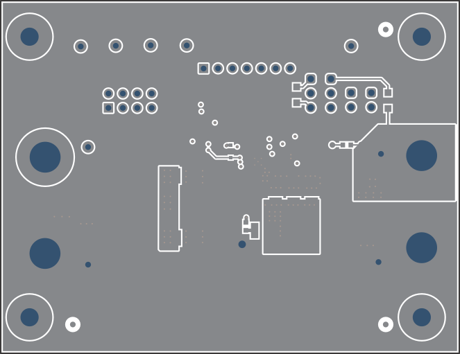 Figure 6-5 Bottom Layer
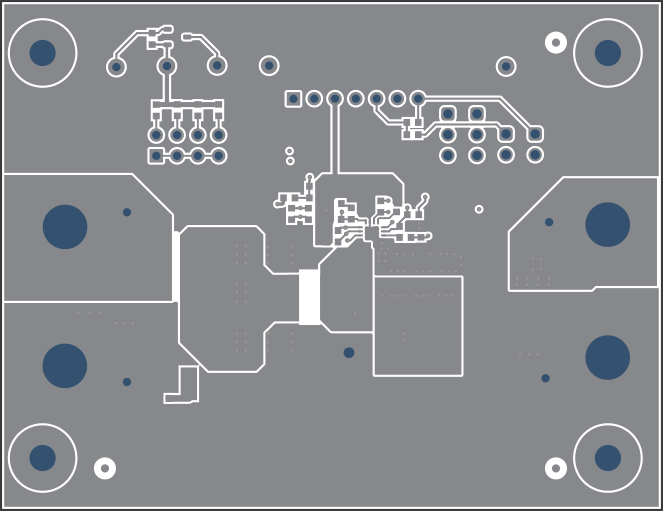 Figure 6-2 Top Layer
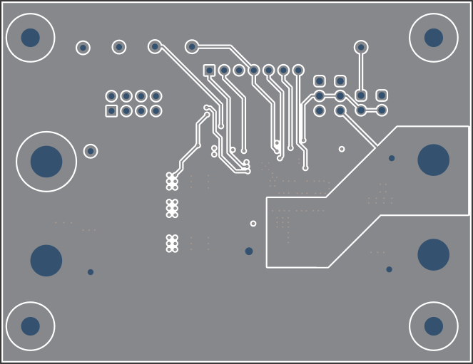 Figure 6-4 Signal Layer 2
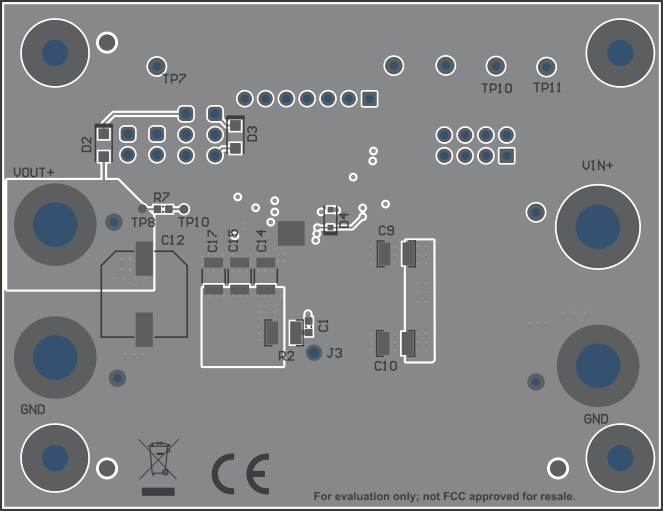 Figure 6-6 Bottom Layer and Silkscreen
(mirrored)