SPRABJ8B September 2022 – November 2023 AM2631 , AM2631-Q1 , AM2632 , AM2632-Q1 , AM2634 , AM2634-Q1 , AM263P4
12.1 Ground Return
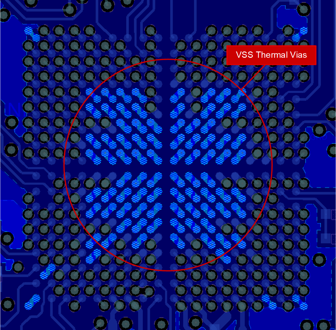
All available ground return BGA must be utilized to create the best possible electrical and thermal connection between the AM263x or AM263Px package and the attached PCB. Maximizing VSS BGA usage is critical from signal integrity, EMI/EMC and thermal perspectives.
Unless a separate top package heatsink is used in the design, the VSS BGA (and VDDCORE to a lesser extent) are the only heat sinking thermal connection for the BGA package. For required, thermal performance, AM263x or AM263Px PCB designs must adhere to following thermal via design requirements.
- A minimum of 49 VSS vias in the center of the BGA must be shorted to PCB ground return planes. However, if possible, and for best thermal performance, all VSS BGA should be connected to PCB ground return planes
- Solid ground return planes shall be used directly under the BGA on as many layers as possible.
- Solid ground return, or the widest possible traces shall be used on the top or bottom mounting layer for VSS BGA pad connection
- VSS via drills shall use largest possible drill diameter. This will maximize surface area of the via, providing lowest thermal resistance.
- VSS vias should be conductively filled, if possible.
All of these thermal via requirements must be balanced against the necessary power and signal fan-out of the design.
The AM263x and AM263Px devices contain both analog and digital ground return pins. Both analog and digital ground return pins should be shorted to a common set of ground return planes on the PCB for best noise and EMI performance as this creates the lowest possible impedance path for all return currents to follow. It is not recommended to separate these two return paths as this typically ends up with lower performance return paths for both digital and analog signal paths.
 Figure 12-1 AM263x controlCARD Excerpt – Ground Return Vias Under AM263x BGA Layer 1 and Layer 2
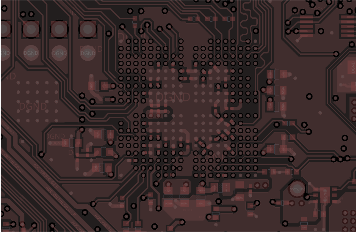
 Figure 12-2 AM263x controlCARD Excerpt – Ground Return Vias Under AM263x BGA Layer 10