SPRABJ8B September 2022 – November 2023 AM2631 , AM2631-Q1 , AM2632 , AM2632-Q1 , AM2634 , AM2634-Q1 , AM263P4
12.3.1 Key Layout Considerations
- Wide 15 mil traces should be used for all power and ground return via fan-out.
- 3.3 V I/O power tends to be shared across multiple devices in the system, recommend routing with very wide power planes across the PCB to minimize IR drops to all components including the AM263x or AM263Px
- A tightly coupled, adjacent ground return reference plane should be used for best transient performance and EMI coupling
- A wide power plane entry that covers the BGA 3.3 V power pin areas should be used for minimal IR drop and best transient performance
- Larger packaged, lower-frequency, bulk capacitance should be placed adjacent to MCU BGA with vias directly to power plane paths
- Smaller packaged, higher-frequency decoupling capacitance should be placed directly on BGA fan-out vias with as small of a dog-bone to power and ground return vias as possible
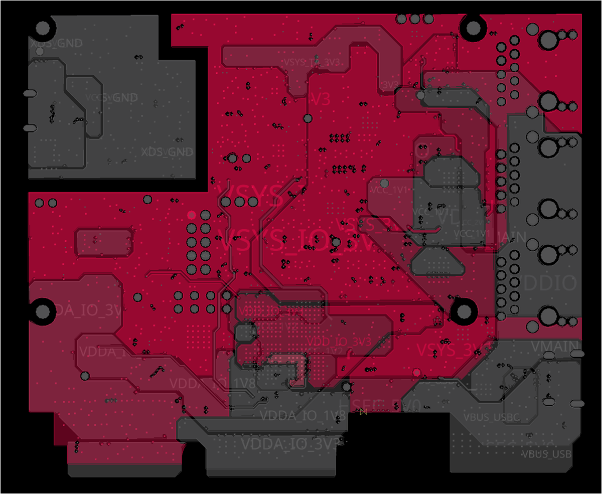 Figure 12-7 AM263x controlCARD Excerpt – 3.3 V Digital and Analog Power Planes on Layer 5 and Layer 6
 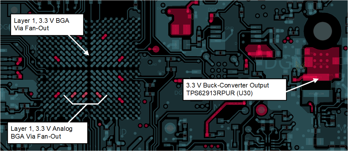 Figure 12-8 AM263x controlCARD Excerpt – 3.3 V Digital I/O and Analog I/O BGA Pinout and Regulator Output
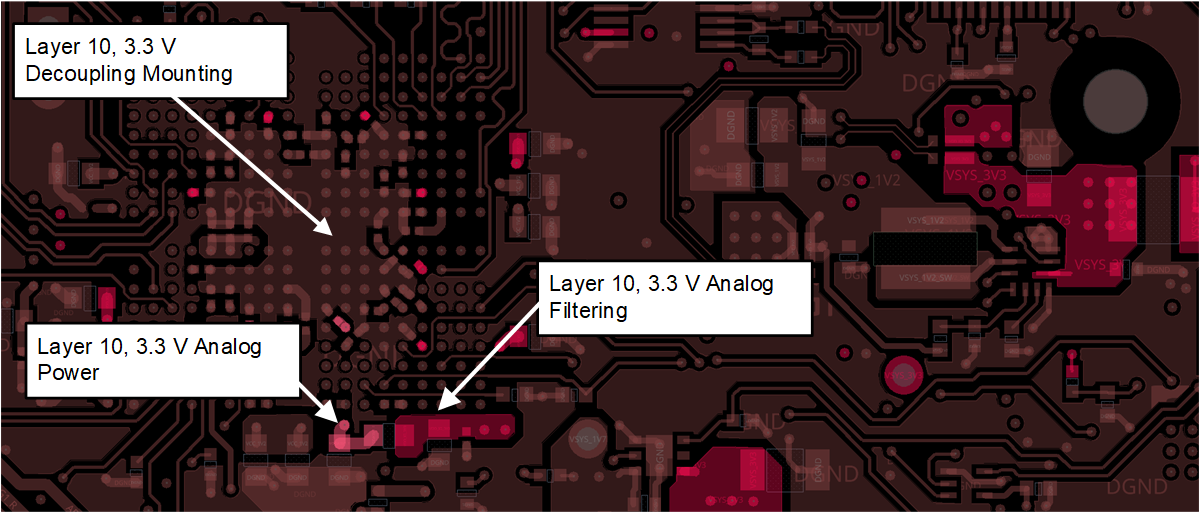 Figure 12-9 AM263x controlCARD Excerpt – Common 3.3 V Plane Transition Vias
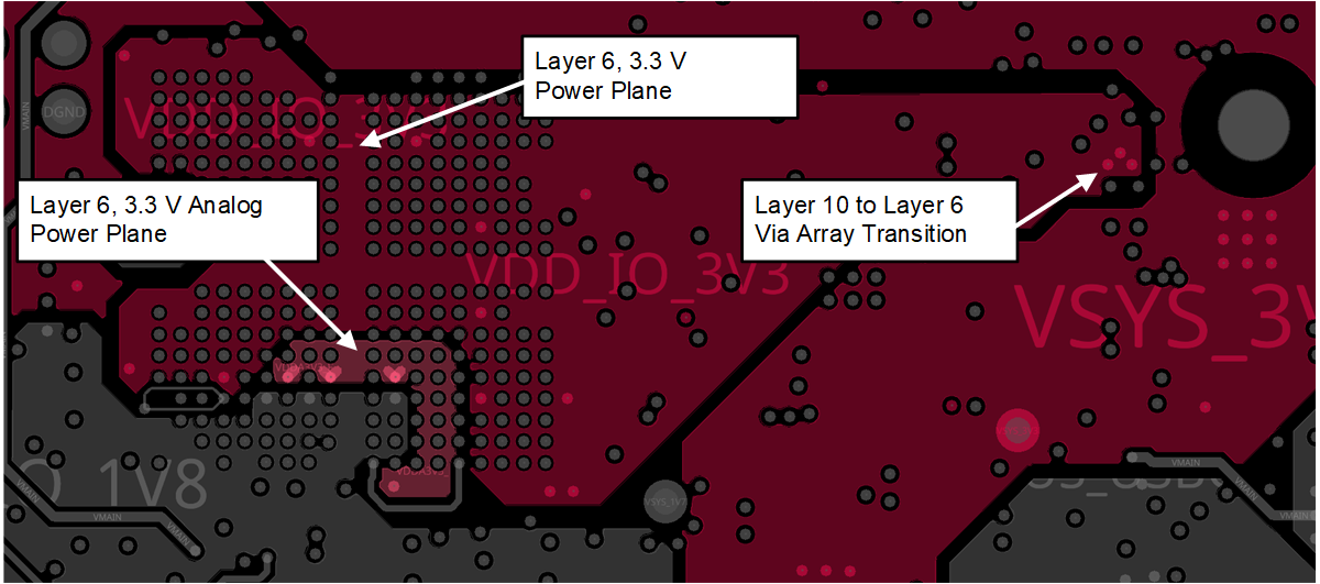 Figure 12-10 AM263x controlCARD Excerpt – 3.3 V Digital and Analog Planes Layer 6
  Figure 12-11 AM263x controlCARD Excerpt – 3.3 V Digital and Analog Power Decoupling Mounting, Layer 10